DM385, DM388
www.ti.com
SPRS821D –MARCH 2013–REVISED DECEMBER 2013
8.13.3.4 Compatible DDR3 Devices
Table 8-61 shows the parameters of the DDR3 devices that are compatible with this interface. Generally,
the interface is compatible with DDR3 devices in the x8 or x16 widths.
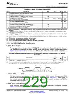
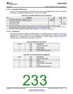
Table 8-61. Compatible DDR3 Devices (Per Interface)
NO.
1
PARAMETER
DDR3 device speed grade: ≤ 400 MHz clock rate(1)
DDR3 device speed grade: > 400 MHz clock rate(1)
DDR3 device bit width
MIN
DDR3-800
DDR3-1600
x8
MAX
UNIT
(2)
(2)
2
3
x16
4
Bits
4
DDR3 device count(3)
2
Devices
(1) DDR3 speed grade depends on desired clock rate. Data rate is 2x the clock rate. For DDR3-800, the clock rate is 400 MHz.
(2) DDR3 devices with higher speed grades are supported; however, max clock rate will still be limited to 533 MHz as stated in Table 8-59
Switching Characteristics Over Recommended Operating Conditions for DDR3 Memory Controller.
(3) For valid DDR3 device configurations and device counts, see Section 8.13.3.3, Figure 8-56, and Figure 8-57.
8.13.3.5 PCB Stackup
The minimum stackup for routing the DDR3 interface is a four-layer stack up as shown in Table 8-62.
Additional layers may be added to the PCB stackup to accommodate other circuitry, enhance SI/EMI
performance, or to reduce the size of the PCB footprint. A six-layer stackup is shown in Table 8-63.
Complete stackup specifications are provided in Table 8-64.
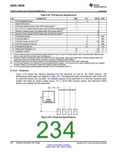
Table 8-62. Minimum PCB Stackup
LAYER
TYPE
Signal
Plane
Plane
Signal
DESCRIPTION
1
2
3
4
Top routing mostly vertical
Split power plane
Full ground plane
Bottom routing mostly horizontal
Table 8-63. Six-Layer PCB Stackup Suggestion
LAYER
TYPE
Signal
Plane
Plane
Plane
Plane
Signal
DESCRIPTION
1
2
3
4
5
6
Top routing mostly vertical
Ground
Split power plane
Split power plane or Internal routing
Ground
Bottom routing mostly horizontal
Copyright © 2013, Texas Instruments Incorporated
Peripheral Information and Timings
233
Submit Documentation Feedback
Product Folder Links: DM385 DM388

 TI [ TEXAS INSTRUMENTS ]