DM385, DM388
SPRS821D –MARCH 2013–REVISED DECEMBER 2013
www.ti.com
UNIT
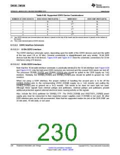
Table 8-64. PCB Stackup Specifications
NO.
1
PARAMETER
MIN
4
TYP
MAX
PCB routing/plane layers
Signal routing layers
6
2
2
3
Full ground reference layers under DDR3 routing region(1)
Full 1.35-V/1.5-V power reference layers under the DDR3 routing region(1)
Number of reference plane cuts allowed within DDR routing region(2)
Number of layers between DDR3 routing layer and reference plane(3)
PCB feature spacing
1
4
1
5
0
0
6
7
4
4
Mils
Mils
Mils
Mils
mm
Ω
8
PCB trace width, w
PCB BGA escape via pad size(4)
9
18
10
0.4
20
10 PCB BGA escape via hole size
11 Processor BGA pad size
13 Single-ended impedance, Zo
14 Impedance control(5)
50
75
Z-5
Z
Z+5
Ω
(1) Ground reference layers are preferred over power reference layers. Be sure to include bypass caps to accommodate reference layer
return current as the trace routes switch routing layers.
(2) No traces should cross reference plane cuts within the DDR routing region. High-speed signal traces crossing reference plane cuts
create large return current paths which can lead to excessive crosstalk and EMI radiation.
(3) Reference planes are to be directly adjacent to the signal plane to minimize the size of the return current loop.
(4) An 18-mil pad assumes Via Channel is the most economical BGA escape. A 20-mil pad may be used if additional layers are available
for power routing. An 18-mil pad is required for minimum layer count escape.
(5) Z is the nominal singled-ended impedance selected for the PCB specified by item 13.
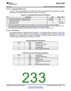
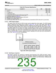
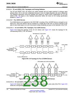
8.13.3.6 Placement
Figure 8-58 shows the required placement for the processor as well as the DDR3 devices. The
dimensions for this figure are defined in Table 8-65. The placement does not restrict the side of the PCB
on which the devices are mounted. The ultimate purpose of the placement is to limit the maximum trace
lengths and allow for proper routing space. For a 16-bit DDR memory system, the high-word DDR3
devices are omitted from the placement.
X1
X2
X2
X2
DDR3
Controller
Y
Figure 8-58. Placement Specifications
234
Peripheral Information and Timings
Copyright © 2013, Texas Instruments Incorporated
Submit Documentation Feedback
Product Folder Links: DM385 DM388

 TI [ TEXAS INSTRUMENTS ]