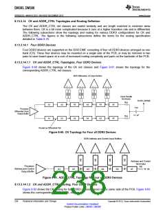
DM385, DM388
www.ti.com
SPRS821D –MARCH 2013–REVISED DECEMBER 2013
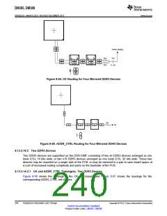
8.13.3.9.1 Return Current Bypass Capacitors
Use additional bypass capacitors if the return current reference plane changes due to DDR3 signals
hopping from one signal layer to another. The bypass capacitor here provides a path for the return current
to hop planes along with the signal. As many of these return current bypass capacitors should be used as
possible. Since these are returns for signal current, the signal via size may be used for these capacitors.
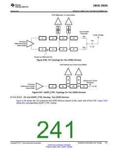
8.13.3.10 Net Classes
Table 8-68 lists the clock net classes for the DDR3 interface. Table 8-69 lists the signal net classes, and
associated clock net classes, for signals in the DDR3 interface. These net classes are used for the
termination and routing rules that follow.
Table 8-68. Clock Net Class Definitions
CLOCK NET CLASS PROCESSOR PIN NAMES
CK
DDR[0]_CLK/DDR[0]_CLK
DQS0
DDR[0]_DQS[0]/DDR[0]_DQS[0]
DDR[0]_DQS[1]/DDR[0]_DQS[1]
DDR[0]_DQS[2]/DDR[0]_DQS[2]
DDR[0]_DQS[3]/DDR[0]_DQS[3]
DQS1
DQS2(1)
DQS3(1)
(1) Only used on 32-bit wide DDR3 memory systems.
Table 8-69. Signal Net Class Definitions
ASSOCIATED CLOCK
PROCESSOR PIN NAMES
NET CLASS
CLOCK NET CLASS
ADDR_CTRL
CK
DDR[0]_BA[2:0], DDR[0]_A[15:0], DDR[0]_CS[x], DDR[0]_CAS,
DDR[0]_RAS, DDR[0]_WE, DDR[0]_CKE, DDR[0]_ODT[0]
DQ0
DQ1
DQ2(1)
DQ3(1)
DQS0
DQS1
DQS2
DQS3
DDR[0]_D[7:0], DDR[0]_DQM[0]
DDR[0]_D[15:8], DDR[0]_DQM[1]
DDR[0]_D[23:16], DDR[0]_DQM[2]
DDR[0]_D[31:24], DDR[0]_DQM[3]
(1) Only used on 32-bit wide DDR3 memory systems.
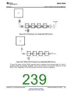
8.13.3.11 DDR3 Signal Termination
Signal terminators are required for the CK and ADDR_CTRL net classes. The data lines are terminated by
ODT and, thus, the PCB traces should be unterminated. Detailed termination specifications are covered in
the routing rules in the following sections.
8.13.3.12 VREFSSTL_DDR Routing
VREFSSTL_DDR (VREF) is used as a reference by the input buffers of the DDR3 memories as well as
the processor. VREF is intended to be half the DDR3 power supply voltage and is typically generated with
the DDR3 1.35-V/1.5-V and VTT power supply. It should be routed as a nominal 20-mil wide trace with 0.1
µF bypass capacitors near each device connection. Narrowing of VREF is allowed to accommodate
routing congestion.
8.13.3.13 VTT
Like VREF, the nominal value of the VTT supply is half the DDR3 supply voltage. Unlike VREF, VTT is
expected to source and sink current, specifically the termination current for the ADDR_CTRL net class
Thevinen terminators. VTT is needed at the end of the address bus and it should be routed as a power
sub-plane. VTT should be bypassed near the terminator resistors.
Copyright © 2013, Texas Instruments Incorporated
Peripheral Information and Timings
237
Submit Documentation Feedback
Product Folder Links: DM385 DM388

 TI [ TEXAS INSTRUMENTS ]