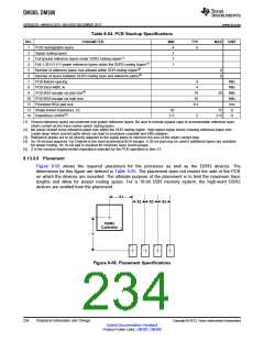
DM385, DM388
SPRS821D –MARCH 2013–REVISED DECEMBER 2013
www.ti.com
8.13.3.14 CK and ADDR_CTRL Topologies and Routing Definition
The CK and ADDR_CTRL net classes are routed similarly and are length matched to minimize skew
between them. CK is a bit more complicated because it runs at a higher transition rate and is differential.
The following subsections show the topology and routing for various DDR3 configurations for CK and
ADDR_CTRL. The figures in the following subsections define the terms for the routing specification
detailed in Table 8-70.
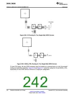
8.13.3.14.1 Four DDR3 Devices
Four DDR3 devices are supported on the DDR EMIF consisting of four x8 DDR3 devices arranged as one
bank (CS). These four devices may be mounted on a single side of the PCB, or may be mirrored in two
pairs to save board space at a cost of increased routing complexity and parts on the backside of the PCB.
8.13.3.14.1.1 CK and ADDR_CTRL Topologies, Four DDR3 Devices
Figure 8-60 shows the topology of the CK net classes and Figure 8-61 shows the topology for the
corresponding ADDR_CTRL net classes.
DDR Differential CK Input Buffers
–
–
–
–
+
+
+
+
Clock Parallel
Terminator
DVDD_DDR[0]
Rcp
A1
A1
A2
A2
A3
A3
A4
A4
A3
A3
AT
AT
Cac
Processor
Differential Clock
Output Buffer
+
–
0.1 µF
Rcp
Routed as Differential Pair
Figure 8-60. CK Topology for Four x8 DDR3 Devices
DDR Address and Control Input Buffers
Address and Control
Terminator
Rtt
Processor
Address and Control
Output Buffer
A1
A2
A3
A4
A3
AT
Vtt
Figure 8-61. ADDR_CTRL Topology for Four x8 DDR3 Devices
8.13.3.14.1.2 CK and ADDR_CTRL Routing, Four DDR3 Devices
Figure 8-62 shows the CK routing for four DDR3 devices placed on the same side of the PCB. Figure 8-63
shows the corresponding ADDR_CTRL routing.
238
Peripheral Information and Timings
Copyright © 2013, Texas Instruments Incorporated
Submit Documentation Feedback
Product Folder Links: DM385 DM388

 TI [ TEXAS INSTRUMENTS ]