DM385, DM388
SPRS821D –MARCH 2013–REVISED DECEMBER 2013
www.ti.com
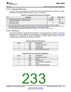
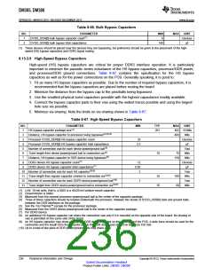
Table 8-66. Bulk Bypass Capacitors
NO.
1
PARAMETER
DVDD_DDR[0] bulk bypass capacitor count(1)
DVDD_DDR[0] bulk bypass total capacitance
MIN
6
MAX
UNIT
Devices
μF
2
140
(1) These devices should be placed near the devices they are bypassing, but preference should be given to the placement of the high-
speed (HS) bypass capacitors and DDR3 signal routing.
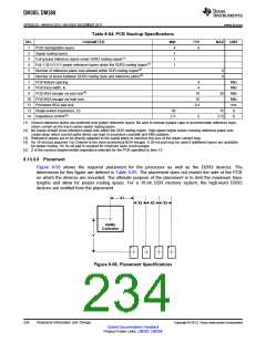
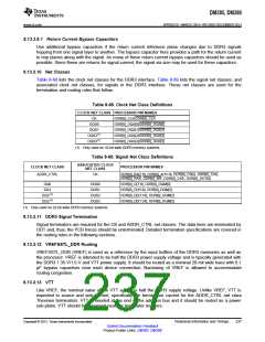
8.13.3.9 High-Speed Bypass Capacitors
High-speed (HS) bypass capacitors are critical for proper DDR3 interface operation. It is particularly
important to minimize the parasitic series inductance of the HS bypass capacitors, processor/DDR power,
and processor/DDR ground connections. Table 8-67 contains the specification for the HS bypass
capacitors as well as for the power connections on the PCB. Generally speaking, it is good to:
1. Fit as many HS bypass capacitors as possible. Due to the number of required bypass capacitors, it is
recommended that the bypass capacitors are placed before routing the board.
2. Minimize the distance from the bypass cap to the pins/balls being bypassed.
3. Use the smallest physical sized capacitors possible with the highest capacitance readily available.
4. Connect the bypass capacitor pads to their vias using the widest traces possible and using the largest
hole size via possible.
5. Minimize via sharing. Note the limits on via sharing shown in Table 8-67.
Table 8-67. High-Speed Bypass Capacitors
NO.
1
PARAMETER
HS bypass capacitor package size(1)
MIN
TYP
MAX
UNIT
201
402 10 Mils
2
Distance, HS bypass capacitor to processor being bypassed(2)(3)(4)
400
Mils
Devices
μF
3
Processor DVDD_DDR[0] HS bypass capacitor count
35
4
Processor DVDD_DDR[0] HS bypass capacitor total capacitance
Number of connection vias for each device power/ground ball(5)
Trace length from device power/ground ball to connection via(2)
Distance, HS bypass capacitor to DDR device being bypassed(6)
DDR3 device HS bypass capacitor count(7)
2.5
5
Vias
Mils
6
35
70
7
150
Mils
8
12
0.85
2
Devices
μF
9
DDR3 device HS bypass capacitor total capacitance(7)
10 Number of connection vias for each HS capacitor(8)(9)
Vias
Mils
11 Trace length from bypass capacitor connect to connection via(2)(9)
12 Number of connection vias for each DDR3 device power/ground ball(10)
13 Trace length from DDR3 device power/ground ball to connection via(2)(8)
35
35
100
60
1
Vias
Mils
(1) LxW, 10-mil units, that is, a 0402 is a 40x20-mil surface-mount capacitor.
(2) Closer/shorter is better.
(3) Measured from the nearest processor power/ground ball to the center of the capacitor package.
(4) Three of these capacitors should be located underneath the processor, between the cluster of DVDD_DDR[0] balls and ground balls,
between the DDR interfaces on the package.
(5) See the Via Channel™ escape for the processor package.
(6) Measured from the DDR3 device power/ground ball to the center of the capacitor package.
(7) Per DDR3 device.
(8) An additional HS bypass capacitor can share the connection vias only if it is mounted on the opposite side of the board. No sharing of
vias is permitted on the same side of the board.
(9) An HS bypass capacitor may share a via with a DDR device mounted on the same side of the PCB. A wide trace should be used for the
connection and the length from the capacitor pad to the DDR device pad should be less than 150 mils.
(10) Up to a total of two pairs of DDR power/ground balls may share a via.
236
Peripheral Information and Timings
Copyright © 2013, Texas Instruments Incorporated
Submit Documentation Feedback
Product Folder Links: DM385 DM388

 TI [ TEXAS INSTRUMENTS ]