DM385, DM388
www.ti.com
NO.
SPRS821D –MARCH 2013–REVISED DECEMBER 2013
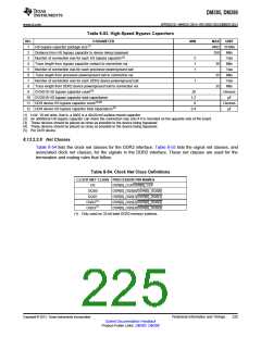
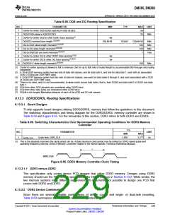
Table 8-58. DQS and DQ Routing Specification
PARAMETER
MIN
TYP
MAX
2w
UNIT
1
2
3
4
5
6
7
8
9
Center-to-center DQS-DQSn spacing in E0|E1|E2|E3
DQS-DQSn skew in E0|E1|E2|E3
Center-to-center DQS to other DDR2 trace spacing(1)
25
Mils
4w
(2)(3)(4)
DQS/DQ nominal trace length
DQ-to-DQS skew length mismatch(2)(3)(4)
DQ-to-DQ skew length mismatch(2)(3)(4)
DQ-to-DQ/DQS via count mismatch(2)(3)(4)
Center-to-center DQ to other DDR2 trace spacing(1)(5)
Center-to-center DQ to other DQ trace spacing(1)(6)(7)
DQLM-50
DQLM
DQLM+50
Mils
Mils
Mils
Vias
100
100
1
4w
3w
10 DQ/DQS E skew length mismatch(2)(3)(4)
100
Mils
(1) Center-to-center spacing is allowed to fall to minimum (2w) for up to 500 mils of routed length to accommodate BGA escape and routing
congestion.
(2) A 16-bit DDR memory system has two sets of data net classes; one for data byte 0, and one for data byte 1, each with an associated
DQS (2 DQSs) per DDR EMIF used.
(3) A 32-bit DDR memory system has four sets of data net classes; one each for data bytes 0 through 3, and each associated with a DQS
(4 DQSs) per DDR EMIF used.
(4) There is no need, and it is not recommended, to skew match across data bytes; that is, from DQS0 and data byte 0 to DQS1 and data
byte 1.
(5) DQs from other DQS domains are considered other DDR2 trace.
(6) DQs from other data bytes are considered other DDR2 trace.
(7) DQLM is the longest Manhattan distance of each of the DQS and DQ net classes.
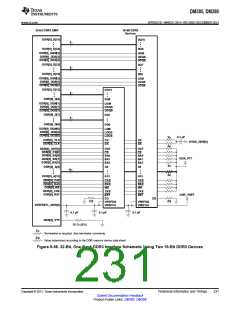
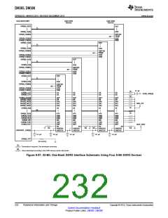
8.13.3 DDR3/DDR3L Routing Specifications
8.13.3.1 Board Designs
TI only supports board designs utilizing DDR3/DDR3L memory that follow the guidelines in this document.
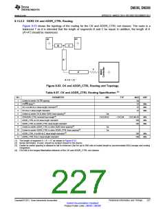
The switching characteristics and timing diagram for the DDR3/DDR3L memory controller are shown in
Table 8-59 and Figure 8-55. For the remainder of this section, DDR3 refers to both DDR3 and DDR3L.
Table 8-59. Switching Characteristics Over Recommended Operating Conditions for DDR3 Memory
Controller
-1G
NO.
PARAMETER
UNIT
MIN
MAX
1
tc(DDR_CLK)
Cycle time, DDR_CLK
1.876
3.3(1)
ns
(1) This is the absolute maximum the clock period can be. Actual maximum clock period may be limited by DDR3 speed grade and
operating frequency (see the DDR2/3 Memory Controller chapter in the device-specific Technical Reference Manual).
1
DDR_CLK
Figure 8-55. DDR3 Memory Controller Clock Timing
8.13.3.1.1 DDR3 versus DDR2
This specification only covers device PCB designs that utilize DDR3 memory. Designs using DDR2
memory should use the PCB design specifications for DDR2 memory in Section 8.13.2. While similar, the
two memory systems have different requirements. It is currently not possible to design one PCB that
covers both DDR2 and DDR3.
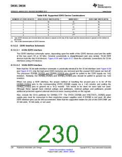
8.13.3.2 DDR3 Device Combinations
Since there are several possible combinations of device counts and single- or dual-side mounting,
Table 8-60 summarizes the supported device configurations.
Copyright © 2013, Texas Instruments Incorporated
Peripheral Information and Timings
229
Submit Documentation Feedback
Product Folder Links: DM385 DM388

 TI [ TEXAS INSTRUMENTS ]