ADS1115-Q1
SBAS563 –DECEMBER 2011
www.ti.com
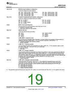
Lo_thresh AND Hi_thresh REGISTERS
A
secondary conversion ready function of the
comparator output pin can be realized by setting the
Hi_thresh register MSB to '1' and the Lo_thresh
register MSB to ‘0’. However, in all other cases, the
Hi_thresh register must be larger than the Lo_thresh
register. The threshold register formats are shown in
Table 10. When set to RDY mode, the ALERT/RDY
pin outputs the OS bit when in single-shot mode and
pulses when in continuous conversion mode.
The upper and lower threshold values used by the
comparator are stored in two 16-bit registers. These
registers store values in the same format that the
output register displays values; that is, they are
stored in twos complement format. Because it is
implemented as
a
digital comparator, special
attention should be taken to readjust values
whenever PGA settings are changed.
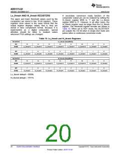
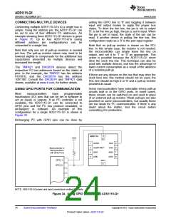
Table 10. Lo_thresh and Hi_thresh Registers
REGISTER
BIT
Lo_thresh (Read/Write)
15
14
13
12
Lo_thresh12
blank
11
10
9
8
NAME
Lo_thresh15
Lo_thresh14
Lo_thresh13
Lo_thresh11
Lo_thresh10
Lo_thresh9
Lo_thresh8
BIT
7
6
5
4
3
2
1
0
NAME
Lo_thresh7
Lo_thresh6
Lo_thresh5
Lo_thresh4
Lo_thresh3
Lo_thresh2
Lo_thresh1
Lo_thresh0
REGISTER
BIT
Hi_thresh (Read/Write)
15
14
13
12
Hi_thresh12
blank
11
10
9
8
NAME
Hi_thresh15
Hi_thresh14
Hi_thresh13
Hi_thresh11
Hi_thresh10
Hi_thresh9
Hi_thresh8
BIT
7
6
5
4
3
2
1
0
NAME
Hi_thresh7
Hi_thresh6
Hi_thresh5
Hi_thresh4
Hi_thresh3
Hi_thresh2
Hi_thresh1
Hi_thresh0
Lo_thresh default = 8000h.
Hi_thresh default = 7FFFh.
20
Submit Documentation Feedback
Copyright © 2011, Texas Instruments Incorporated
Product Folder Link(s) :ADS1115-Q1

 TI [ TEXAS INSTRUMENTS ]