ADS1115-Q1
SBAS563 –DECEMBER 2011
www.ti.com
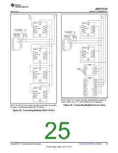
CONNECTING MULTIPLE DEVICES
setting the GPIO line to '0' and toggling it between
input and output modes to apply the proper bus
states. To drive the line low, the pin is set to output
'0'; to let the line go high, the pin is set to input. When
the pin is set to input, the state of the pin can be
read; if another device is pulling the line low, this
configuration reads as a '0' in the port input register.
Connecting multiple ADS1115-Q1s to a single bus is
simple. Using the address pin, the ADS1115-Q1 can
be set to one of four different I2C addresses. An
example showing three ADS1115-Q1 devices is given
in Figure 35. Up to four ADS1115-Q1s (using
different address pin configurations) can be
connected to a single bus.
Note that no pull-up resistor is shown on the SCL
line. In this simple case, the resistor is not needed;
the microcontroller can simply leave the line on
output, and set it to '1' or '0' as appropriate. This
action is possible because the ADS1115-Q1 never
drive the clock line low. This technique can also be
used with multiple devices, and has the advantage of
lower current consumption as a result of the absence
of a resistive pull-up.
Note that only one set of pull-up resistors is needed
per bus. The pull-up resistor values may need to be
lowered slightly to compensate for the additional bus
capacitance presented by multiple devices and
increased line length.
The TMP421 and DAC8574 devices detect the
respective I2C bus addresses based on the states of
pins. In the example, the TMP421 has the address
0101010, and the DAC8574 has the address
1001100. Consult the DAC8574 and TMP421 data
sheets, available at www.ti.com, for further details.
If there are any devices on the bus that may drive the
clock lines low, this method should not be used; the
SCL line should be high-Z or '0' and a pull-up resistor
provided as usual.
Some microcontrollers have selectable strong pull-up
circuits built in to the GPIO ports. In some cases,
these circuits can be switched on and used in place
of an external pull-up resistor. Weak pull-ups are also
provided on some microcontrollers, but usually these
are too weak for I2C communication. If there is any
doubt about the matter, test the circuit before
committing it to production.
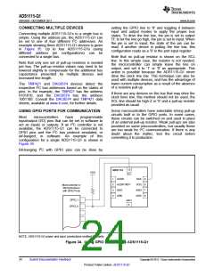
USING GPIO PORTS FOR COMMUNICATION
Most
microcontrollers
have
programmable
input/output (I/O) pins that can be set in software to
act as inputs or outputs. If an I2C controller is not
available, the ADS1115-Q1 can be connected to
GPIO pins and the I2C bus protocol simulated, or
bit-banged, in software. An example of this
configuration for a single ADS1115-Q1 is shown in
Figure 34.
Bit-banging I2C with GPIO pins can be done by
10
ADS1115
VDD
SCL
1
2
3
4
ADDR
SDA
VDD
AIN3
AIN2
9
8
7
6
ALERT/RDY
GND
Microcontroller or
Microprocessor
with GPIO Ports
AIN0
GPIO_1
GPIO_0
AIN1
5
NOTE: ADS1115-Q1 power and input connections omitted for clarity.
Figure 34. Using GPIO with a Single ADS1115-Q1
24
Submit Documentation Feedback
Copyright © 2011, Texas Instruments Incorporated
Product Folder Link(s) :ADS1115-Q1

 TI [ TEXAS INSTRUMENTS ]