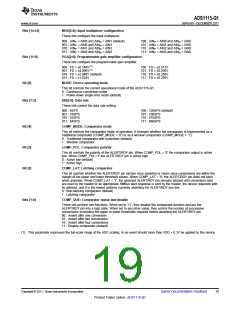
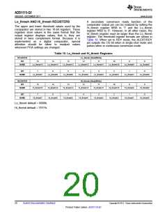
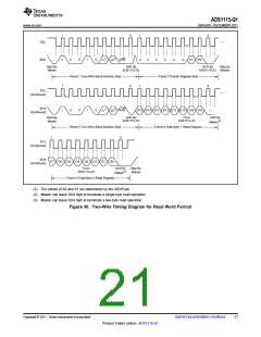
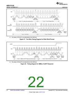
ADS1115-Q1
www.ti.com
SBAS563 –DECEMBER 2011
APPLICATION INFORMATION
The following sections give example circuits and
suggestions for using the ADS1115-Q1 in various
situations.
The ADS1115-Q1 interface directly to standard mode,
fast mode, and high-speed mode I2C controllers. Any
microcontroller I2C peripheral, including master-only
and non-multiple-master I2C peripherals, can operate
with the ADS1115-Q1. The ADS1115-Q1 does not
perform clock-stretching (that is, it never pulls the
clock line low), so it is not necessary to provide for
this function unless other clock-stretching devices are
on the same I2C bus.
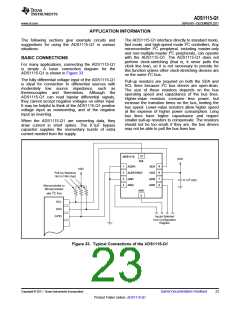
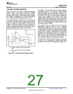
BASIC CONNECTIONS
For many applications, connecting the ADS1115-Q1
is simple. A basic connection diagram for the
ADS1115-Q1 is shown in Figure 33.
The fully differential voltage input of the ADS1115-Q1
is ideal for connection to differential sources with
moderately low source impedance, such as
thermocouples and thermistors. Although the
ADS1115-Q1 can read bipolar differential signals,
they cannot accept negative voltages on either input.
It may be helpful to think of the ADS1115-Q1 positive
voltage input as noninverting, and of the negative
input as inverting.
Pull-up resistors are required on both the SDA and
SCL lines because I2C bus drivers are open-drain.
The size of these resistors depends on the bus
operating speed and capacitance of the bus lines.
Higher-value resistors consume less power, but
increase the transition times on the bus, limiting the
bus speed. Lower-value resistors allow higher speed
at the expense of higher power consumption. Long
bus lines have higher capacitance and require
smaller pull-up resistors to compensate. The resistors
should not be too small; if they are, the bus drivers
may not be able to pull the bus lines low.
When the ADS1115-Q1 are converting data, they
draw current in short spikes. The 0.1μF bypass
capacitor supplies the momentary bursts of extra
current needed from the supply.
10
ADS1115
VDD
SCL
1
2
3
4
ADDR
SDA
VDD
AIN3
AIN2
9
8
7
6
VDD
ALERT/RDY
GND
Pull-Up Resistors
1kW to 10kW (typ)
0.1mF (typ)
AIN0
Microcontroller or
Microprocessor
with I2C Port
AIN1
5
SCL
SDA
GPIO
Inputs Selected
from Configuration
Register
Figure 33. Typical Connections of the ADS1115-Q1
Copyright © 2011, Texas Instruments Incorporated
Submit Documentation Feedback
23
Product Folder Link(s) :ADS1115-Q1

 TI [ TEXAS INSTRUMENTS ]