ADS1115-Q1
SBAS563 –DECEMBER 2011
www.ti.com
1
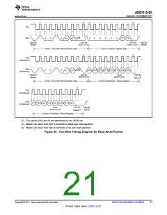
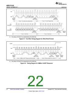
9
1
9
SCL
¼
¼
A1(1) A0(1)
SDA
1
0
0
1
0
R/W
0
0
0
0
0
0
P1
P0
Start By
Master
ACK By
ADS1115-Q1
ACK By
ADS1115-Q1
Frame 2 Pointer Register Byte
Frame 1 Two-Wire Slave Address Byte
1
9
1
9
SCL
(Continued)
SDA
D15 D14 D13 D12 D11 D10 D9
D8
D7
D6
D5
D4
D3
D2
D1
D0
(Continued)
ACK By
ADS1115-Q1
ACK By
ADS1115-Q1
Stop By
Master
Frame 3 Data Byte 1
Frame 4 Data Byte 2
(1) The values of A0 and A1 are determined by the ADDR pin.
Figure 31. Two-Wire Timing Diagram for Write Word Format
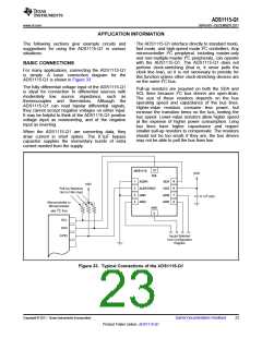
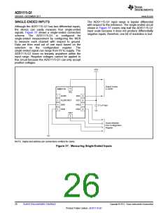
ALERT
SCL
1
9
1
9
SDA
0
0
0
1
1
0
0
R/W
1
0
0
1
A1
A0 Status
Start By
Master
ACK By
ADS1115-Q1
From
ADS1115-Q1
NACK By Stop By
Master Master
Frame 1 SMBus ALERT Response Address Byte
Frame 2 Slave Address From ADS1115
(1) The values of A0 and A1 are determined by the ADDR pin.
Figure 32. Timing Diagram for SMBus ALERT Response
22
Submit Documentation Feedback
Copyright © 2011, Texas Instruments Incorporated
Product Folder Link(s) :ADS1115-Q1

 TI [ TEXAS INSTRUMENTS ]