ADS1115-Q1
www.ti.com
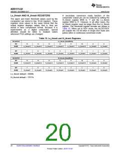
Bits [14:12]
SBAS563 –DECEMBER 2011
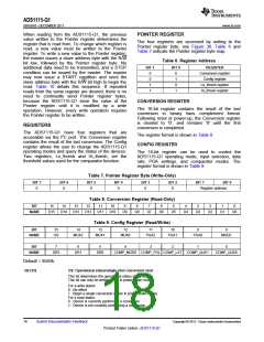
MUX[2:0]: Input multiplexer configuration
These bits configure the input multiplexer.
000 : AINP = AIN0 and AINN = AIN1 (default)
001 : AINP = AIN0 and AINN = AIN3
010 : AINP = AIN1 and AINN = AIN3
011 : AINP = AIN2 and AINN = AIN3
100 : AINP = AIN0 and AINN = GND
101 : AINP = AIN1 and AINN = GND
110 : AINP = AIN2 and AINN = GND
111 : AINP = AIN3 and AINN = GND
Bits [11:9]
PGA[2:0]: Programmable gain amplifier configuration
These bits configure the programmable gain amplifier.
000 : FS = ±6.144V(1)
001 : FS = ±4.096V(1)
010 : FS = ±2.048V (default)
011 : FS = ±1.024V
100 : FS = ±0.512V
101 : FS = ±0.256V
110 : FS = ±0.256V
111 : FS = ±0.256V
Bit [8]
MODE: Device operating mode
This bit controls the current operational mode of the ADS1115-Q1.
0 : Continuous conversion mode
1 : Power-down single-shot mode (default)
Bits [7:5]
DR[2:0]: Data rate
These bits control the data rate setting.
000 : 8SPS
001 : 16SPS
010 : 32SPS
011 : 64SPS
100 : 128SPS (default)
101 : 250SPS
110 : 475SPS
111 : 860SPS
Bit [4]
Bit [3]
Bit [2]
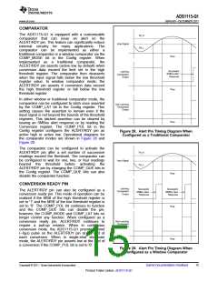
COMP_MODE: Comparator mode
This bit controls the comparator mode of operation. It changes whether the comparator is implemented as a
traditional comparator (COMP_MODE = '0') or as a window comparator (COMP_MODE = '1').
0 : Traditional comparator with hysteresis (default)
1 : Window comparator
COMP_POL: Comparator polarity
This bit controls the polarity of the ALERT/RDY pin. When COMP_POL = '0' the comparator output is active
low. When COMP_POL='1' the ALERT/RDY pin is active high.
0 : Active low (default)
1 : Active high
COMP_LAT: Latching comparator
This bit controls whether the ALERT/RDY pin latches once asserted or clears once conversions are within the
margin of the upper and lower threshold values. When COMP_LAT = '0', the ALERT/RDY pin does not latch
when asserted. When COMP_LAT = '1', the asserted ALERT/RDY pin remains latched until conversion data
are read by the master or an appropriate SMBus alert response is sent by the master, the device responds with
its address, and it is the lowest address currently asserting the ALERT/RDY bus line.
0 : Non-latching comparator (default)
1 : Latching comparator
Bits [1:0]
COMP_QUE: Comparator queue and disable
These bits perform two functions. When set to '11', they disable the comparator function and put the
ALERT/RDY pin into a high state. When set to any other value, they control the number of successive
conversions exceeding the upper or lower thresholds required before asserting the ALERT/RDY pin.
00 : Assert after one conversion
01 : Assert after two conversions
10 : Assert after four conversions
11 : Disable comparator (default)
(1) This parameter expresses the full-scale range of the ADC scaling. In no event should more than VDD + 0.3V be applied to this device.
Copyright © 2011, Texas Instruments Incorporated
Submit Documentation Feedback
19
Product Folder Link(s) :ADS1115-Q1

 TI [ TEXAS INSTRUMENTS ]