ADS1115-Q1
SBAS563 –DECEMBER 2011
www.ti.com
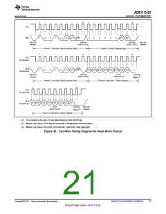
When reading from the ADS1115-Q1, the previous
value written to the Pointer register determines the
register that is read from. To change which register is
read, a new value must be written to the Pointer
register. To write a new value to the Pointer register,
the master issues a slave address byte with the R/W
bit low, followed by the Pointer register byte. No
additional data need to be transmitted, and a STOP
condition can be issued by the master. The master
may now issue a START condition and send the
slave address byte with the R/W bit high to begin the
read. Table 10 details this sequence. If repeated
reads from the same register are desired, there is no
need to continually send Pointer register bytes,
because the ADS1115-Q1 store the value of the
Pointer register until it is modified by a write
operation. However, every write operation requires
the Pointer register to be written.
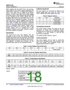
POINTER REGISTER
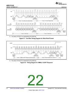
The four registers are accessed by writing to the
Pointer register byte; see Figure 30. Table 6 and
Table 7 indicate the Pointer register byte map.
Table 6. Register Address
BIT 1
BIT 0
REGISTER
0
0
1
1
0
1
0
1
Conversion register
Config register
Lo_thresh register
Hi_thresh register
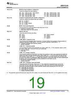
CONVERSION REGISTER
The 16-bit register contains the result of the last
conversion in binary twos complement format.
Following reset or power-up, the Conversion register
is cleared to '0', and remains '0' until the first
conversion is completed.
REGISTERS
The ADS1115-Q1 have four registers that are
accessible via the I2C port. The Conversion register
contains the result of the last conversion. The Config
register allows the user to change the ADS1115-Q1
operating modes and query the status of the devices.
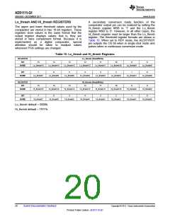
Two registers, Lo_thresh and Hi_thresh, set the
threshold values used for the comparator function.
The register format is shown in Table 8.
CONFIG REGISTER
The 16-bit register can be used to control the
ADS1115-Q1 operating mode, input selection, data
rate, PGA settings, and comparator modes. The
register format is shown in Table 9.
Table 7. Pointer Register Byte (Write-Only)
BIT 7
BIT 6
BIT 5
BIT 4
BIT 3
BIT 2
BIT 1
BIT 0
0
0
0
0
0
0
Register address
Table 8. Conversion Register (Read-Only)
BIT
15
14
13
12
11
10
9
8
7
6
5
4
3
2
1
0
NAME
D15
D14
D13
D12
D11
D10
D9
D8
D7
D6
D5
D4
D3
D2
D1
D0
Table 9. Config Register (Read/Write)
BIT
15
14
13
12
11
10
9
8
NAME
OS
MUX2
MUX1
MUX0
PGA2
PGA1
PGA0
MODE
blank
BIT
7
6
5
4
3
2
1
0
NAME
DR2
DR1
DR0
COMP_MODE COMP_POL COMP_LAT COMP_QUE1
COMP_QUE0
Default = 8583h.
Bit [15]
OS: Operational status/single-shot conversion start
This bit determines the operational status of the device.
This bit can only be written when in power-down mode.
For a write status:
0 : No effect
1 : Begin a single conversion (when in power-down mode)
For a read status:
0 : Device is currently performing a conversion
1 : Device is not currently performing a conversion
18
Submit Documentation Feedback
Copyright © 2011, Texas Instruments Incorporated
Product Folder Link(s) :ADS1115-Q1

 TI [ TEXAS INSTRUMENTS ]