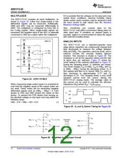
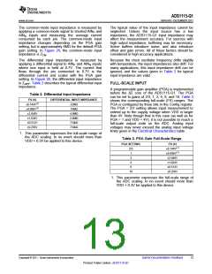
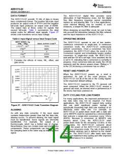
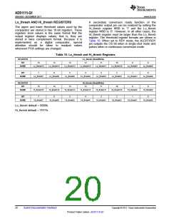
ADS1115-Q1
SBAS563 –DECEMBER 2011
www.ti.com
SMBus ALERT RESPONSE
An I2C bus consists of two lines, SDA and SCL. SDA
carries data; SCL provides the clock. All data are
transmitted across the I2C bus in groups of eight bits.
To send a bit on the I2C bus, the SDA line is driven to
the appropriate level while SCL is low (a low on SDA
indicates the bit is zero; a high indicates the bit is
one). Once the SDA line settles, the SCL line is
brought high, then low. This pulse on SCL clocks the
SDA bit into the receiver shift register. If the I2C bus
is held idle for more than 25ms, the bus times out.
The I2C bus is bidirectional: the SDA line is used for
both transmitting and receiving data. When the
master reads from a slave, the slave drives the data
line; when the master sends to a slave, the master
drives the data line. The master always drives the
clock line. The ADS1115-Q1 never drive SCL,
because they cannot act as a master. On the
ADS1115-Q1, SCL is an input only.
When configured in latching mode (COMP_LAT = '1'
in the Config register), the ALERT/RDY pin can be
implemented with an SMBus alert. The pin asserts if
the comparator detects a conversion that exceeds an
upper or lower threshold. This interrupt is latched and
can be cleared only by reading conversion data, or by
issuing a successful SMBus alert response and
reading the asserting device I2C address. If
conversion data exceed the upper or lower thresholds
after being cleared, the pin reasserts. This assertion
does not affect conversions that are already in
progress. The ALERT/RDY pin, as with the SDA pin,
is an open-drain pin. This architecture allows several
devices to share the same interface bus. When
disabled, the pin holds a high state so that it does not
interfere with other devices on the same bus line.
When the master senses that the ALERT/RDY pin
has latched, it issues an SMBus alert command
(00011001) to the I2C bus. Any ADS1115-Q1 data
converters on the I2C bus with the ALERT/RDY pins
asserted respond to the command with the slave
address. In the event that two or more ADS1115-Q1
data converters present on the bus assert the latched
ALERT/RDY pin, arbitration during the address
response portion of the SMBus alert decides which
device clears its assertion. The device with the lowest
I2C address always wins arbitration. If a device loses
arbitration, it does not clear the comparator output pin
assertion. The master then repeats the SMBus alert
response until all devices have had the respective
assertions cleared. In window comparator mode, the
SMBus alert status bit indicates a '1' if signals exceed
the high threshold and a '0' if signals exceed the low
threshold.
Most of the time the bus is idle; no communication
occurs, and both lines are high. When communication
is taking place, the bus is active. Only master devices
can start a communication and initiate a START
condition on the bus. Normally, the data line is only
allowed to change state while the clock line is low. If
the data line changes state while the clock line is
high, it is either a START condition or a STOP
condition. A START condition occurs when the clock
line is high and the data line goes from high to low. A
STOP condition occurs when the clock line is high
and the data line goes from low to high.
After the master issues a START condition, it sends a
byte that indicates which slave device it wants to
communicate with. This byte is called the address
byte. Each device on an I2C bus has a unique 7-bit
address to which it responds. The master sends an
address in the address byte, together with a bit that
indicates whether it wishes to read from or write to
the slave device.
Every byte transmitted on the I2C bus, whether it is
address or data, is acknowledged with an
acknowledge bit. When the master has finished
sending a byte (eight data bits) to a slave, it stops
driving SDA and waits for the slave to acknowledge
the byte. The slave acknowledges the byte by pulling
SDA low. The master then sends a clock pulse to
clock the acknowledge bit. Similarly, when the master
has finished reading a byte, it pulls SDA low to
acknowledge this to the slave. It then sends a clock
pulse to clock the bit. (The master always drives the
clock line.)
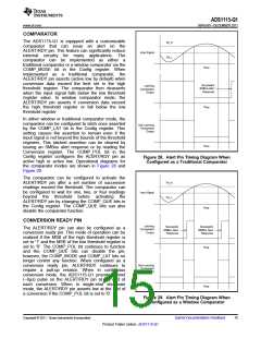
I2C INTERFACE
The ADS1115-Q1 communicate through an I2C
interface. I2C is a two-wire open-drain interface that
supports multiple devices and masters on a single
bus. Devices on the I2C bus only drive the bus lines
low by connecting them to ground; they never drive
the bus lines high. Instead, the bus wires are pulled
high by pull-up resistors, so the bus wires are high
when no device is driving them low. This way, two
devices cannot conflict; if two devices drive the bus
simultaneously, there is no driver contention.
Communication on the I2C bus always takes place
between two devices, one acting as the master and
the other as the slave. Both masters and slaves can
read and write, but slaves can only do so under the
direction of the master. Some I2C devices can act as
masters or slaves, but the ADS1115-Q1 can only act
as slave devices.
A not-acknowledge is performed by simply leaving
SDA high during an acknowledge cycle. If a device is
not present on the bus, and the master attempts to
address it, it receives a not-acknowledge because no
device is present at that address to pull the line low.
16
Submit Documentation Feedback
Copyright © 2011, Texas Instruments Incorporated
Product Folder Link(s) :ADS1115-Q1

 TI [ TEXAS INSTRUMENTS ]