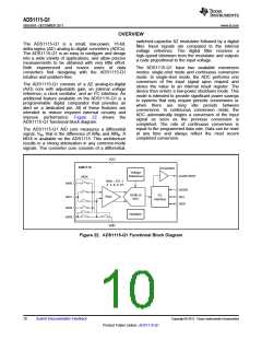
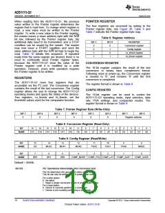
ADS1115-Q1
SBAS563 –DECEMBER 2011
www.ti.com
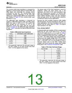
DATA FORMAT
The ADS1115-Q1 digital filter provides some
attenuation of high-frequency noise, but the digital
Sinc filter frequency response cannot completely
replace an anti-aliasing filter. For a few applications,
some external filtering may be needed; in such
instances, a simple RC filter is adequate.
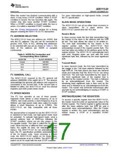
The ADS1115-Q1 provide 16 bits of data in binary
twos complement format. The positive full-scale input
produces an output code of 7FFFh and the negative
full-scale input produces an output code of 8000h.
The output clips at these codes for signals that
exceed full-scale. Table 4 summarizes the ideal
output codes for different input signals. Figure 27
shows code transitions versus input voltage.
When designing an input filter circuit, be sure to take
into account the interaction between the filter network
and the input impedance of the ADS1115-Q1.
Table 4. Input Signal versus Ideal Output Code
OPERATING MODES
INPUT SIGNAL, VIN
The ADS1115-Q1 operate in one of two modes:
continuous conversion or single-shot. In continuous
conversion mode, the ADS1115-Q1 continuously
perform conversions. Once a conversion has been
completed, the ADS1115-Q1 place the result in the
Conversion register and immediately begins another
conversion. In single-shot mode, the ADS1115-Q1
wait until the OS bit is set high. Once asserted, the bit
is set to '0', indicating that a conversion is currently in
progress. Once conversion data are ready, the OS bit
reasserts and the device powers down. Writing a '1'
to the OS bit during a conversion has no effect.
(AINP – AINN)
≥ FS (215 – 1)/215
+FS/215
IDEAL OUTPUT CODE(1)
7FFFh
0001h
0
0
–FS/215
FFFFh
8000h
≤ –FS
1. Excludes the effects of noise, INL, offset, and
gain errors.
0x7FFF
0x7FFE
RESET AND POWER-UP
When the ADS1115-Q1 powers up, a reset is
performed. As part of the reset process, the
ADS1115-Q1 set all of the bits in the Config register
to the respective default settings.
0x0001
0x0000
0xFFFF
The ADS1115-Q1 respond to the I2C general call
reset command. When the ADS1115-Q1 receive a
general call reset, an internal reset is performed as if
the device had been powered on.
0x8001
0x8000
¼
¼
-FS
-FS
0
FS
DUTY CYCLING FOR LOW POWER
Input Voltage (AINP - AINN)
215 - 1
215 - 1
For many applications, the improved performance at
low data rates may not be required. For these
applications, the ADS1115-Q1 support duty cycling
that can yield significant power savings by
periodically requesting high data rate readings at an
effectively lower data rate. For example, an
ADS1115-Q1 in power-down mode with a data rate
set to 860SPS could be operated by a microcontroller
that instructs a single-shot conversion every 125ms
(8SPS). Because a conversion at 860SPS only
requires about 1.2ms, the ADS1115-Q1 enter
power-down mode for the remaining 123.8ms. In this
configuration, the ADS1115-Q1 consume about
1/100th the power of the ADS1115-Q1 operated in
continuous conversion mode. The rate of duty cycling
is completely arbitrary and is defined by the master
controller. The ADS1115-Q1 offer lower data rates
that do not implement duty cycling and offer improved
noise performance if it is needed.
FS
215
215
Figure 27. ADS1115-Q1 Code Transition Diagram
ALIASING
As with any data converter, if the input signal
contains frequencies greater than half the data rate,
aliasing occurs. To prevent aliasing, the input signal
must be bandlimited. Some signals are inherently
bandlimited. For example, the output of
a
thermocouple, which has a limited rate of change.
Nevertheless, they can contain noise and interference
components. These components can fold back into
the sampling band in the same way as with any other
signal.
14
Submit Documentation Feedback
Copyright © 2011, Texas Instruments Incorporated
Product Folder Link(s) :ADS1115-Q1

 TI [ TEXAS INSTRUMENTS ]