ADS1115-Q1
SBAS563 –DECEMBER 2011
www.ti.com
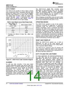
MULTIPLEXER
If it is possible that the voltages on the input pins may
violate these conditions, external Schottky clamp
diodes and/or series resistors may be required to limit
the input current to safe values (see the Absolute
Maximum Ratings table).
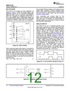
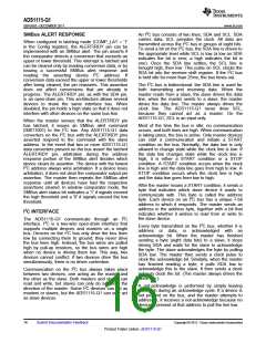
The ADS1115-Q1 contains an input multiplexer, as
shown in Figure 24. Either four single-ended or two
differential signals can be measured. Additionally,
AIN0 and AIN1 may be measured differentially to
AIN3. The multiplexer is configured by three bits in
the Config register. When single-ended signals are
measured, the negative input of the ADC is internally
connected to GND by a switch within the multiplexer.
Also, overdriving one unused input on the
ADS1115-Q1 may affect conversions taking place on
other input pins. If overdrive on unused inputs is
possible, again it is recommended to clamp the signal
with external Schottky diodes.
VDD
ADS1115
ANALOG INPUTS
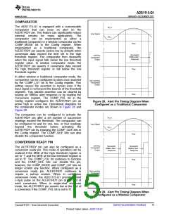
The ADS1115-Q1 use a switched-capacitor input
stage where capacitors are continuously charged and
then discharged to measure the voltage between
AINP and AINN. The capacitors used are small, and to
external circuitry the average loading appears
resistive. This structure is shown in Figure 26. The
resistance is set by the capacitor values and the rate
at which they are switched. Figure 25 shows the
on/off setting of the switches illustrated in Figure 26.
During the sampling phase, S1 switches are closed.
This event charges CA1 to AINP, CA2 to AINN, and CB
to (AINP – AINN). During the discharge phase, S1 is
first opened and then S2 is closed. Both CA1 and CA2
then discharge to approximately 0.7V and CB
discharges to 0V. This charging draws a very small
transient current from the source driving the
ADS1115-Q1 analog inputs. The average value of
this current can be used to calculate the effective
AIN0
VDD
AINP
AINN
GND
VDD
AIN1
AIN2
AIN3
GND
VDD
GND
GND
GND
Figure 24. ADS1115 MUX
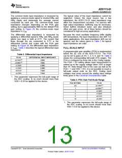
When measuring single-ended inputs it is important to
note that the negative range of the output codes are
not used. These codes are for measuring negative
differential signals such as (AINP – AINN) < 0. ESD
diodes to VDD and GND protect the inputs on this
device. To prevent the ESD diodes from turning on,
the absolute voltage on any input must stay within the
following range:
impedance (Reff) where Reff = VIN/IAVERAGE
.
tSAMPLE
ON
S1
OFF
ON
S2
OFF
GND – 0.3V < AINx < VDD + 0.3V
(1)
Figure 25. S1 and S2 Switch Timing for Figure 26
0.7V
CA1
ZCM
Equivalent
Circuit
AINP
0.7V
0.7V
AINP
S1
S2
S2
CB
ZDIFF
S1
AINN
AINN
ZCM
CA2
f
= 250kHz
CLK
0.7V
Figure 26. Simplified Analog Input Circuit
12
Submit Documentation Feedback
Copyright © 2011, Texas Instruments Incorporated
Product Folder Link(s) :ADS1115-Q1

 TI [ TEXAS INSTRUMENTS ]