ADS1115-Q1
www.ti.com
SBAS563 –DECEMBER 2011
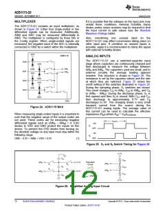
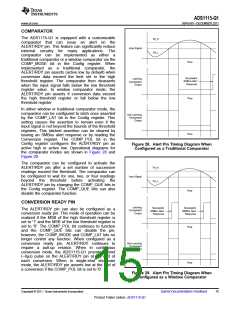
The common-mode input impedance is measured by
applying a common-mode signal to shorted AINP and
AINN inputs and measuring the average current
consumed by each pin. The common-mode input
impedance changes depending on the PGA gain
setting, but is approximately 6MΩ for the default PGA
gain setting. In Figure 26, the common-mode input
The typical value of the input impedance cannot be
neglected. Unless the input source has a low
impedance, the ADS1115-Q1 input impedance may
affect the measurement accuracy. For sources with
high output impedance, buffering may be necessary.
Active buffers introduce noise, and also introduce
offset and gain errors. All of these factors should be
considered in high-accuracy applications.
impedance is ZCM
.
The differential input impedance is measured by
applying a differential signal to AINP and AINN inputs
where one input is held at 0.7V. The current that
flows through the pin connected to 0.7V is the
differential current and scales with the PGA gain
setting. In Figure 26, the differential input impedance
is ZDIFF. Table 2 describes the typical differential input
impedance.
Because the clock oscillator frequency drifts slightly
with temperature, the input impedances also drift. For
many applications, this input impedance drift can be
ignored, and the values given in Table 2 for typical
input impedance are valid.
FULL-SCALE INPUT
A programmable gain amplifier (PGA) is implemented
before the ΔΣ core of the ADS1115-Q1. The PGA
can be set to gains of 2/3, 1, 2, 4, 8, and 16. Table 3
shows the corresponding full-scale (FS) ranges. The
PGA is configured by three bits in the Config register.
The PGA = 2/3 setting allows input measurement to
extend up to the supply voltage when VDD is larger
than 4V. Note though that in this case (as well as for
PGA = 1 and VDD < 4V), it is not possible to reach a
full-scale output code on the ADC. Analog input
voltages may never exceed the analog input voltage
limits given in the Electrical Characteristics table.
Table 2. Differential Input Impedance
FS (V)
±6.144V(1)
±4.096V(1)
±2.048V
±1.024V
±0.512V
±0.256V
DIFFERENTIAL INPUT IMPEDANCE
22MΩ
15MΩ
4.9MΩ
2.4MΩ
710kΩ
710kΩ
1. This parameter expresses the full-scale range of
the ADC scaling. In no event should more than
VDD + 0.3V be applied to this device.
Table 3. PGA Gain Full-Scale Range
PGA SETTING
FS (V)
±6.144V(1)
±4.096V(1)
±2.048V
±1.024V
±0.512V
±0.256V
2/3
1
2
4
8
16
1. This parameter expresses the full-scale range of
the ADC scaling. In no event should more than
VDD + 0.3V be applied to this device.
Copyright © 2011, Texas Instruments Incorporated
Submit Documentation Feedback
13
Product Folder Link(s) :ADS1115-Q1

 TI [ TEXAS INSTRUMENTS ]