ADS1115-Q1
www.ti.com
SBAS563 –DECEMBER 2011
QUICKSTART GUIDE
For example, to write to the configuration register to
set the ADS1115-Q1 to continuous conversion mode
and then read the conversion result, send the
following bytes in this order:
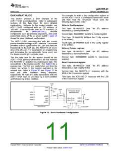
This section provides
a brief example of the
ADS1115-Q1 communications. Refer to subsequent
sections of this data sheet for more detailed
explanations. Hardware for this design includes: one
ADS1115-Q1 configured with an I2C address of
1001000; a microcontroller with an I2C interface (TI
Write to Config register:
First byte: 0b10010000 (first 7-bit I2C address
followed by a low read/write bit)
recommends
the
MSP430F2002);
discrete
components such as resistors, capacitors, and serial
connectors; and a 2V to 5V power supply. Figure 23
shows the basic hardware configuration.
Second byte: 0b00000001 (points to Config register)
Third byte: 0b10000100 (MSB of the Config register
to be written)
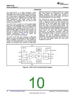
The ADS1115-Q1 communicates with the master
(microcontroller) through an I2C interface. The master
provides a clock signal on the SCL pin and data are
transferred via the SDA pin. The ADS1115-Q1 never
drives the SCL pin. For information on programming
and debugging the microcontroller being used, see
the device-specific product data sheet.
Fourth byte: 0b10000011 (LSB of the Config register
to be written)
Write to Pointer register:
First byte: 0b10010000 (first 7-bit I2C address
followed by a low read/write bit)
Second byte: 0b00000000 (points to Conversion
register)
The first byte sent by the master should be the
ADS1115-Q1 address followed by a bit that instructs
the ADS1115-Q1 to listen for a subsequent byte. The
second byte is the register pointer. See Table 9 for a
register map. The third and fourth bytes sent from the
master are written to the register indicated in the
second byte. Refer to Figure 30 and Figure 31 for
read and write operation timing diagrams,
respectively. All read and write transactions with the
ADS1115-Q1 must be preceded by a start condition
and followed by a stop condition.
Read Conversion register:
First byte: 0b10010001 (first 7-bit I2C address
followed by a high read/write bit)
Second byte: the ADS1115-Q1 response with the
MSB of the Conversion register
Third byte: the ADS1115-Q1 response with the LSB
of the Conversion register
+3.3V
VDD
100nF
GND
+3.3V
I2C-Capable Master
(MSP430F2002)
AIN0
AIN1
+3.3V
10kW
10kW
ADDR
AIN2
VDD
GND
SCL
SCL (P1.6)
SDA (P1.7)
AIN3
100nF
SDA
ALERT
ADS1115-Q1
Serial/UART
JTAG
Figure 23. Basic Hardware Configuration
Copyright © 2011, Texas Instruments Incorporated
Submit Documentation Feedback
11
Product Folder Link(s) :ADS1115-Q1

 TI [ TEXAS INSTRUMENTS ]