UPSD3212C, UPSD3212CV
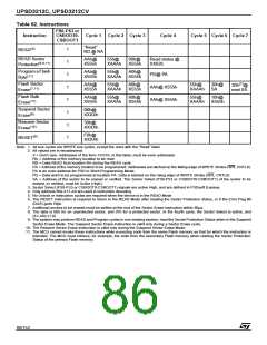
Programming Flash Memory
Flash memory must be erased prior to being pro-
grammed. A byte of Flash memory is erased to all
'1s' (FFh), and is programmed by setting selected
bits to '0.' The MCU may erase Flash memory all
at once or by-sector, but not byte-by-byte. Howev-
er, the MCU may program Flash memory byte-by-
byte.
The primary and secondary Flash memories re-
quire the MCU to send an instruction to program a
byte or to erase sectors (see Table 62).
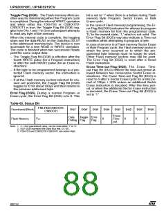
Once the MCU issues a Flash memory Program or
Erase instruction, it must check for the status bits
for completion. The embedded algorithms that are
invoked support several means to provide status
to the MCU. Status may be checked using any of
three methods: Data Polling, Data Toggle, or
Ready/Busy (PC3).
byte that was written to the Flash memory with the
byte that was intended to be written.
When using the Data Polling method during an
Erase cycle, Figure 42 still applies. However, the
Data Polling Flag Bit (DQ7) is '0' until the Erase cy-
cle is complete. A '1' on the Error Flag Bit (DQ5) in-
dicates a time-out condition on the Erase cycle; a
'0' indicates no error. The MCU can read any loca-
tion within the sector being erased to get the Data
Polling Flag Bit (DQ7) and the Error Flag Bit
(DQ5).
PSDsoft Express generates ANSI C code func-
tions which implement these Data Polling algo-
rithms.
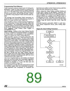
Figure 42. Data Polling Flowchart
Data Polling. Polling on the Data Polling Flag Bit
(DQ7) is a method of checking whether a Program
or Erase cycle is in progress or has completed.
Figure 42 shows the Data Polling algorithm.
START
READ DQ5 & DQ7
at VALID ADDRESS
When the MCU issues a Program instruction, the
embedded algorithm begins. The MCU then reads
the location of the byte to be programmed in Flash
memory to check status. The Data Polling Flag Bit
(DQ7) of this location becomes the complement of
b7 of the original data byte to be programmed. The
MCU continues to poll this location, comparing the
Data Polling Flag Bit (DQ7) and monitoring the Er-
ror Flag Bit (DQ5). When the Data Polling Flag Bit
(DQ7) matches b7 of the original data, and the Er-
ror Flag Bit (DQ5) remains '0,' the embedded algo-
rithm is complete. If the Error Flag Bit (DQ5) is '1,'
the MCU should test the Data Polling Flag Bit
(DQ7) again since the Data Polling Flag Bit (DQ7)
may have changed simultaneously with the Error
Flag Bit (DQ5) (see Figure 42).
DQ7
=
YES
DATA
NO
NO
DQ5
= 1
YES
READ DQ7
DQ7
=
DATA
YES
The Error Flag Bit (DQ5) is set if either an internal
time-out occurred while the embedded algorithm
attempted to program the byte or if the MCU at-
tempted to program a '1' to a bit that was not
erased (not erased is logic '0').
NO
FAIL
PASS
It is suggested (as with all Flash memories) to read
the location again after the embedded program-
ming algorithm has completed, to compare the
AI01369B
89/152

 STMICROELECTRONICS [ ST ]