UPSD3212C, UPSD3212CV
SRAM
The SRAM is enabled when SRAM Select (RS0)
from the DPLD is High. SRAM Select (RS0) can
contain up to two product terms, allowing flexible
memory mapping.
The SRAM can be backed up using an external
battery. The external battery should be connected
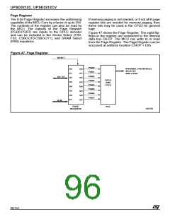
lap, priority is given to the secondary Flash
memory sector.
6. SRAM, I/O, and Peripheral I/O spaces may
overlap any other memory sector. Priority is giv-
en to the SRAM, I/O, or Peripheral I/O.
Example. FS0 is valid when the address is in the
range of 8000h to BFFFh, CSBOOT0 is valid from
8000h to 9FFFh, and RS0 is valid from 8000h to
87FFh. Any address in the range of RS0 always
accesses the SRAM. Any address in the range of
CSBOOT0 greater than 87FFh (and less than
9FFFh) automatically addresses secondary Flash
memory segment 0. Any address greater than
9FFFh accesses the primary Flash memory seg-
ment 0. You can see that half of the primary Flash
memory segment 0 and one-fourth of secondary
Flash memory segment 0 cannot be accessed in
this example.
to Voltage Standby (V
, PC2). If you have an
STBY
external battery connected to the uPSD3200, the
contents of the SRAM are retained in the event of
a power loss. The contents of the SRAM are re-
tained so long as the battery voltage remains at 2V
or greater. If the supply voltage falls below the bat-
tery voltage, an internal power switchover to the
battery occurs.
PC4 can be configured as an output that indicates
when power is being drawn from the external bat-
tery. Battery-on Indicator (V
, PC4) is High
BATON
with the supply voltage falls below the battery volt-
age and the battery on Voltage Standby (V
PC2) is supplying power to the internal SRAM.
,
STBY
Note: An equation that defined FS1 to anywhere
in the range of 8000h to BFFFh would not be valid.
SRAM Select (RS0), Voltage Standby (V
,
STBY
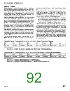
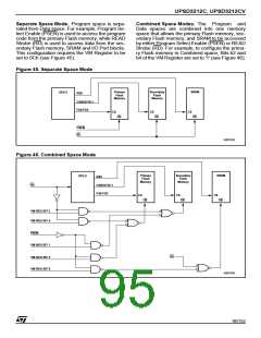
Figure 44 shows the priority levels for all memory
components. Any component on a higher level can
overlap and has priority over any component on a
lower level. Components on the same level must
not overlap. Level one has the highest priority and
level 3 has the lowest.
PC2) and Battery-on Indicator (V
, PC4) are
BATON
all configured using PSDsoft Express Configura-
tion.
Sector Select and SRAM Select
Sector Select (FS0-FS3, CSBOOT0-CSBOOT1)
and SRAM Select (RS0) are all outputs of the
DPLD. They are setup by writing equations for
them in PSDsoft Express. The following rules ap-
ply to the equations for these signals:
Figure 44. Priority Level of Memory and I/O
Components in the PSD MODULE
1. Primary Flash memory and secondary Flash
memory Sector Select signals must not be larg-
er than the physical sector size.
2. Any primary Flash memory sector must not be
mapped in the same memory space as another
Flash memory sector.
3. A secondary Flash memory sector must not be
mapped in the same memory space as another
secondary Flash memory sector.
4. SRAM, I/O, and Peripheral I/O spaces must not
overlap.
Highest Priority
Level 1
SRAM, I/O, or
Peripheral I/O
Level 2
Secondary
Non-Volatile Memory
Level 3
Primary Flash Memory
Lowest Priority
AI02867D
5. A secondary Flash memory sector may overlap
a primary Flash memory sector. In case of over-
93/152

 STMICROELECTRONICS [ ST ]