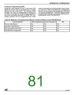
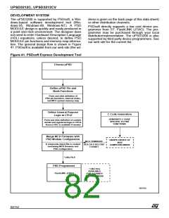
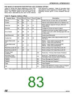
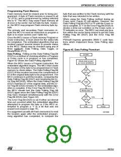
UPSD3212C, UPSD3212CV
Instructions
An instruction consists of a sequence of specific
operations. Each received byte is sequentially de-
coded by the PSD MODULE and not executed as
a standard WRITE operation. The instruction is ex-
ecuted when the correct number of bytes are prop-
erly received and the time between two
consecutive bytes is shorter than the time-out pe-
riod. Some instructions are structured to include
READ operations after the initial WRITE opera-
tions.
The instruction must be followed exactly. Any in-
valid combination of instruction bytes or time-out
between two consecutive bytes while addressing
Flash memory resets the device logic into READ
Mode (Flash memory is read like a ROM device).
These instructions are detailed in Table 62. For ef-
ficient decoding of the instructions, the first two
bytes of an instruction are the coded cycles and
are followed by an instruction byte or confirmation
byte. The coded cycles consist of writing the data
AAh to address X555h during the first cycle and
data 55h to address XAAAh during the second cy-
cle. Address signals A15-A12 are Don’t Care dur-
ing the instruction WRITE cycles. However, the
appropriate
Sector
Select
(FS0-FS3
or
CSBOOT0-CSBOOT1) must be selected.
The primary and secondary Flash memories have
the same instruction set. The Sector Select signals
determine which Flash memory is to receive and
execute the instruction. The primary Flash memo-
ry is selected if any one of Sector Select (FS0-
FS3) is High, and the secondary Flash memory is
selected if any one of Sector Select (CSBOOT0-
CSBOOT1) is High.
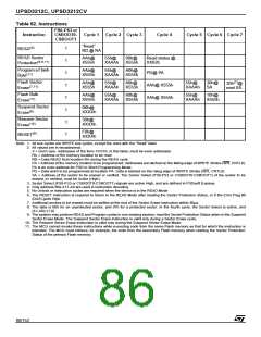
The Flash memory supports the instructions sum-
marized in Table 62:
Flash memory:
■ Erase memory by chip or sector
■ Suspend or resume sector erase
■ Program a Byte
■ RESET to READ Mode
■ Read Sector Protection Status
85/152

 STMICROELECTRONICS [ ST ]