UPSD3212C, UPSD3212CV
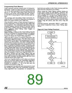
Toggle Flag (DQ6). The Flash memory offers an-
other way for determining when the Program cycle
is completed. During the internal WRITE operation
and when either the FS0-FS3 or CSBOOT0-
CSBOOT1 is true, the Toggle Flag Bit (DQ6) tog-
gles from 0 to 1 and 1 to 0 on subsequent attempts
to read any byte of the memory.
When the internal cycle is complete, the toggling
stops and the data READ on the Data Bus D0-D7
is the addressed memory byte. The device is now
accessible for a new READ or WRITE operation.
The cycle is finished when two successive Reads
yield the same output data.
– The Toggle Flag Bit (DQ6) is effective after the
fourth WRITE pulse (for a Program instruction)
or after the sixth WRITE pulse (for an Erase in-
struction).
– If the byte to be programmed belongs to a pro-
tected Flash memory sector, the instruction is
ignored.
bit is set to '1' when there is a failure during Flash
memory Byte Program, Sector Erase, or Bulk
Erase cycle.
In the case of Flash memory programming, the Er-
ror Flag Bit (DQ5) indicates the attempt to program
a Flash memory bit from the programmed state,
'0,' to the erased state, '1,' which is not valid. The
Error Flag Bit (DQ5) may also indicate a Time-out
condition while attempting to program a byte.
In case of an error in a Flash memory Sector Erase
or Byte Program cycle, the Flash memory sector in
which the error occurred or to which the pro-
grammed byte belongs must no longer be used.
Other Flash memory sectors may still be used.
The Error Flag Bit (DQ5) is reset after a Reset
Flash instruction.
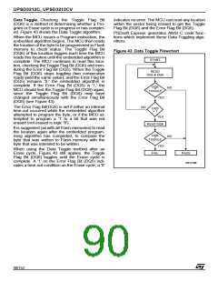
Erase Time-out Flag (DQ3). The Erase Time-
out Flag Bit (DQ3) reflects the time-out period al-
lowed between two consecutive Sector Erase in-
structions. The Erase Time-out Flag Bit (DQ3) is
reset to 0 after a Sector Erase cycle for a time pe-
riod of 100µs + 20% unless an additional Sector
Erase instruction is decoded. After this time peri-
od, or when the additional Sector Erase instruction
is decoded, the Erase Time-out Flag Bit (DQ3) is
set to '1.'
– If all the Flash memory sectors selected for era-
sure are protected, the Toggle Flag Bit (DQ6)
toggles to '0' for about 100µs and then returns to
the previous addressed byte.
Error Flag (DQ5). During a normal Program or
Erase cycle, the Error Flag Bit (DQ5) is to 0. This
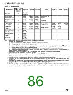
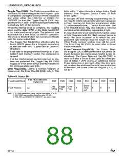
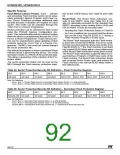
Table 63. Status Bit
FS0-FS3/CSBOOT0-
Functional Block
DQ7
DQ6
DQ5
DQ4
DQ3
DQ2
DQ1
DQ0
CSBOOT1
Erase
Time-
out
Data
Polling Flag
Toggle Error
Flag
V
Flash Memory
X
X
X
X
IH
Note: 1. X = Not guaranteed value, can be read either '1' or '0.'
2. DQ7-DQ0 represent the Data Bus bits, D7-D0.
3. FS0-FS3 and CSBOOT0-CSBOOT1 are active High.
88/152

 STMICROELECTRONICS [ ST ]