UPSD3212C, UPSD3212CV
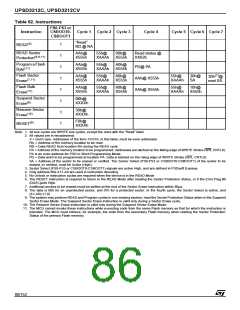
Table 62. Instructions
FS0-FS3 or
Instruction
CSBOOT0-
Cycle 1
Cycle 2 Cycle 3
Cycle 4
Cycle 5 Cycle 6 Cycle 7
CSBOOT1
“Read”
RD @ RA
(5)
1
1
1
1
1
1
1
1
READ
READ Sector
AAh@
X555h
55h@
XAAAh
90h@
X555h
Read status @
XX02h
(6,8,11)
Protection
Program a Flash
AAh@
X555h
55h@
XAAAh
A0h@
X555h
PD@ PA
(11)
Byte
(7)
Flash Sector
AAh@
X555h
55h@
XAAAh
80h@
X555h
55h@
XAAAh
30h@
SA
30h
@
AAh@ X555h
AAh@ X555h
(7,11)
Erase
next SA
Flash Bulk
AAh@
X555h
55h@
XAAAh
80h@
X555h
55h@
XAAAh
10h@
X555h
(11)
Erase
Suspend Sector
B0h@
XXXXh
(9)
Erase
Resume Sector
30h@
XXXXh
(10)
Erase
F0h@
XXXXh
(6)
RESET
Note: 1. All bus cycles are WRITE bus cycles, except the ones with the “Read” label
2. All values are in hexadecimal:
X = Don’t care. Addresses of the form XXXXh, in this table, must be even addresses
RA = Address of the memory location to be read
RD = Data READ from location RA during the READ cycle
PA = Address of the memory location to be programmed. Addresses are latched on the falling edge of WRITE Strobe (WR, CNTL0).
PA is an even address for PSD in Word Programming Mode.
PD = Data word to be programmed at location PA. Data is latched on the rising edge of WRITE Strobe (WR, CNTL0)
SA = Address of the sector to be erased or verified. The Sector Select (FS0-FS3 or CSBOOT0-CSBOOT1) of the sector to be
erased, or verified, must be Active (High).
3. Sector Select (FS0-FS3 or CSBOOT0-CSBOOT1) signals are active High, and are defined in PSDsoft Express.
4. Only address Bits A11-A0 are used in instruction decoding.
5. No Unlock or instruction cycles are required when the device is in the READ Mode
6. The RESET Instruction is required to return to the READ Mode after reading the Sector Protection Status, or if the Error Flag Bit
(DQ5) goes High.
7. Additional sectors to be erased must be written at the end of the Sector Erase instruction within 80µs.
8. The data is 00h for an unprotected sector, and 01h for a protected sector. In the fourth cycle, the Sector Select is active, and
(A1,A0)=(1,0)
9. The system may perform READ and Program cycles in non-erasing sectors, read the Sector Protection Status when in the Suspend
Sector Erase Mode. The Suspend Sector Erase instruction is valid only during a Sector Erase cycle.
10. The Resume Sector Erase instruction is valid only during the Suspend Sector Erase Mode.
11. The MCU cannot invoke these instructions while executing code from the same Flash memory as that for which the instruction is
intended. The MCU must retrieve, for example, the code from the secondary Flash memory when reading the Sector Protection
Status of the primary Flash memory.
86/152

 STMICROELECTRONICS [ ST ]