UPSD3212C, UPSD3212CV
Specific Features
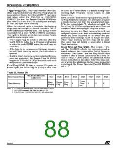
Flash Memory Sector Protect. Each
primary
ters (in the CSIOP block). See Table 64 and Table
65.
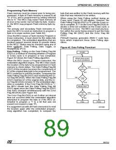
Reset Flash. The Reset Flash instruction con-
sists of one WRITE cycle (see Table 62). It can
also be optionally preceded by the standard two
WRITE decoding cycles (writing AAh to 555h and
55h to AAAh). It must be executed after:
and secondary Flash memory sector can be sepa-
rately protected against Program and Erase cy-
cles. Sector Protection provides additional data
security because it disables all Program or Erase
cycles. This mode can be activated through the
JTAG Port or a Device Programmer.
Sector protection can be selected for each sector
using the PSDsoft Express Configuration pro-
gram. This automatically protects selected sectors
when the device is programmed through the JTAG
Port or a Device Programmer. Flash memory sec-
tors can be unprotected to allow updating of their
contents using the JTAG Port or a Device Pro-
grammer. The MCU can read (but cannot change)
the sector protection bits.
Any attempt to program or erase a protected Flash
memory sector is ignored by the device. The Verify
operation results in a READ of the protected data.
This allows a guarantee of the retention of the Pro-
tection status.
– Reading the Flash Protection Status or Flash ID
– An Error condition has occurred (and the device
has set the Error Flag Bit (DQ5) to '1' during a
Flash memory Program or Erase cycle.
The Reset Flash instruction puts the Flash memo-
ry back into normal READ Mode. If an Error condi-
tion has occurred (and the device has set the Error
Flag Bit (DQ5) to '1' the Flash memory is put back
into normal READ Mode within a few milliseconds
of the Reset Flash instruction having been issued.
The Reset Flash instruction is ignored when it is is-
sued during a Program or Bulk Erase cycle of the
Flash memory. The Reset Flash instruction aborts
any on-going Sector Erase cycle, and returns the
Flash memory to the normal READ Mode within a
few milliseconds.
The sector protection status can be read by the
MCU through the Flash memory protection regis-
Table 64. Sector Protection/Security Bit Definition – Flash Protection Register
Bit 7
Bit 6
Bit 5
Bit 4
Bit 3
Bit 2
Bit 1
Bit 0
not used
not used
not used
not used
Sec3_Prot
Sec2_Prot
Sec1_Prot
Sec0_Prot
Note: Bit Definitions:
Sec<i>_Prot 1 = Primary Flash memory or secondary Flash memory Sector <i> is write-protected.
Sec<i>_Prot 0 = Primary Flash memory or secondary Flash memory Sector <i> is not write-protected.
Table 65. Sector Protection/Security Bit Definition – Secondary Flash Protection Register
Bit 7
Bit 6
Bit 5
Bit 4
Bit 3
Bit 2
Bit 1
Bit 0
Security_Bit not used
Note: Bit Definitions:
not used
not used
not used
not used
Sec1_Prot
Sec0_Prot
Sec<i>_Prot 1 = Secondary Flash memory Sector <i> is write-protected.
Sec<i>_Prot 0 = Secondary Flash memory Sector <i> is not write-protected.
Security_Bit 0 = Security Bit in device has not been set; 1 = Security Bit in device has been set.
92/152

 STMICROELECTRONICS [ ST ]