UPSD3212C, UPSD3212CV
Power-down Instruction and Power-up Mode
Power-up Mode. The PSD MODULE internal
logic is reset upon Power-up to the READ Mode.
Sector Select (FS0-FS3 and CSBOOT0-
CSBOOT1) must be held Low, and WRITE Strobe
(WR, CNTL0) High, during Power-up for maximum
security of the data contents and to remove the
possibility of a byte being written on the first edge
of WRITE Strobe (WR, CNTL0). Any WRITE cycle
the section entitled “Flash Memory Sector Pro-
tect,” page 92, for register definitions.
Reading the Erase/Program Status Bits. The
Flash memory provides several status bits to be
used by the MCU to confirm the completion of an
Erase or Program cycle of Flash memory. These
status bits minimize the time that the MCU spends
performing these tasks and are defined in Table
63, page 88. The status bits can be read as many
times as needed.
initiation is locked when V is below V
.
CC
LKO
READ
Under typical conditions, the MCU may read the
primary Flash memory or the secondary Flash
memory using READ operations just as it would a
ROM or RAM device. Alternately, the MCU may
use READ operations to obtain status information
about a Program or Erase cycle that is currently in
progress. Lastly, the MCU may use instructions to
read special data from these memory blocks. The
following sections describe these READ functions.
READ Memory Contents. Primary Flash memo-
ry and secondary Flash memory are placed in the
READ Mode after Power-up, chip reset, or a
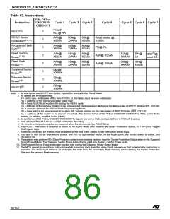
Reset Flash instruction (see Table 62, page 86).
The MCU can read the memory contents of the pri-
mary Flash memory or the secondary Flash mem-
ory by using READ operations any time the READ
operation is not part of an instruction.
READ Memory Sector Protection Status. The
primary Flash memory Sector Protection Status is
read with an instruction composed of 4 operations:
3 specific WRITE operations and a READ opera-
tion (see Table 62). During the READ operation,
address Bits A6, A1, and A0 must be '0,' '1,' and
'0,' respectively, while Sector Select (FS0-FS3 or
CSBOOT0-CSBOOT1) designates the Flash
memory sector whose protection has to be veri-
fied. The READ operation produces 01h if the
Flash memory sector is protected, or 00h if the
sector is not protected.
For Flash memory, the MCU can perform a READ
operation to obtain these status bits while an
Erase or Program instruction is being executed by
the embedded algorithm. See the section entitled
“Programming Flash Memory,” page 89, for de-
tails.
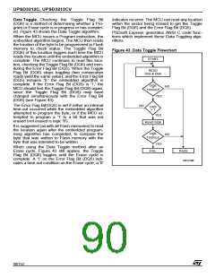
Data Polling Flag (DQ7). When erasing or pro-
gramming in Flash memory, the Data Polling Flag
Bit (DQ7) outputs the complement of the bit being
entered for programming/writing on the DQ7 Bit.
Once the Program instruction or the WRITE oper-
ation is completed, the true logic value is read on
the Data Polling Flag Bit (DQ7) (in a READ opera-
tion).
– Data Polling is effective after the fourth WRITE
pulse (for a Program instruction) or after the
sixth WRITE pulse (for an Erase instruction). It
must be performed at the address being pro-
grammed or at an address within the Flash
memory sector being erased.
– During an Erase cycle, the Data Polling Flag Bit
(DQ7) outputs a '0.' After completion of the cy-
cle, the Data Polling Flag Bit (DQ7) outputs the
last bit programmed (it is a '1' after erasing).
– If the byte to be programmed is in a protected
Flash memory sector, the instruction is ignored.
– If all the Flash memory sectors to be erased are
protected, the Data Polling Flag Bit (DQ7) is re-
set to '0' for about 100µs, and then returns to the
previous addressed byte. No erasure is per-
formed.
The sector protection status for all NVM blocks
(primary Flash memory or secondary Flash mem-
ory) can also be read by the MCU accessing the
Flash Protection registers in PSD I/O space. See
87/152

 STMICROELECTRONICS [ ST ]