UPSD3212C, UPSD3212CV
PSD MODULE DETAILED OPERATION
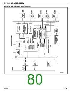
As shown in Figure 15, the PSD MODULE con-
sists of five major types of functional blocks:
Memory Block Select Signals
The DPLD generates the Select signals for all the
internal memory blocks (see the section entitled
“PLDs,” page 97). Each of the eight sectors of the
primary Flash memory has a Select signal (FS0-
FS3) which can contain up to three product terms.
Each of the 2 sectors of the secondary Flash
■ Memory Block
■ PLD Blocks
■ I/O Ports
■ Power Management Unit (PMU)
■ JTAG Interface
memory has
a
Select signal (CSBOOT0-
CSBOOT1) which can contain up to three product
terms. Having three product terms for each Select
signal allows a given sector to be mapped in Pro-
gram or Data space.
The functions of each block are described in the
following sections. Many of the blocks perform
multiple functions, and are user configurable.
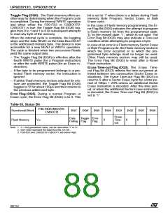
Ready/Busy (PC3). This signal can be used to
output the Ready/Busy status of the Flash memo-
ry. The output on Ready/Busy (PC3) is a 0 (Busy)
when Flash memory is being written to, or when
Flash memory is being erased. The output is a 1
(Ready) when no WRITE or Erase cycle is in
progress.
Memory Operation. The primary Flash memory
and secondary Flash memory are addressed
through the MCU Bus. The MCU can access these
memories in one of two ways:
MEMORY BLOCKS
The PSD MODULE has the following memory
blocks:
■ Primary Flash memory
■ Secondary Flash memory
■ SRAM
The Memory Select signals for these blocks origi-
nate from the Decode PLD (DPLD) and are user-
defined in PSDsoft Express.
– The MCU can execute a typical bus WRITE or
READ operation.
– The MCU can execute a specific Flash memory
instruction that consists of several WRITE and
READ operations. This involves writing specific
data patterns to special addresses within the
Flash memory to invoke an embedded algo-
rithm. These instructions are summarized in Ta-
ble 62.
Primary Flash Memory and Secondary Flash
memory Description
The primary Flash memory is divided into 4 sec-
tors (16KBytes each). The secondary Flash mem-
ory is divided into 2 sectors (8KBytes each). Each
sector of either memory block can be separately
protected from Program and Erase cycles.
Typically, the MCU can read Flash memory using
READ operations, just as it would read a ROM de-
vice. However, Flash memory can only be altered
using specific Erase and Program instructions. For
example, the MCU cannot write a single byte di-
rectly to Flash memory as it would write a byte to
RAM. To program a byte into Flash memory, the
MCU must execute a Program instruction, then
test the status of the Program cycle. This status
test is achieved by a READ operation or polling
Ready/Busy (PC3).
Flash memory may be erased on a sector-by-sec-
tor basis. Flash sector erasure may be suspended
while data is read from other sectors of the block
and then resumed after reading.
During a Program or Erase cycle in Flash memory,
the status can be output on Ready/Busy (PC3).
This pin is set up using PSDsoft Express Configu-
ration.
84/152

 STMICROELECTRONICS [ ST ]