UPSD3212C, UPSD3212CV
PLD Power Management
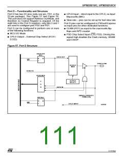
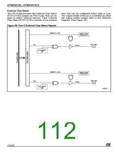
PSD Chip Select Input (CSI, PD2)
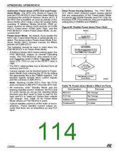
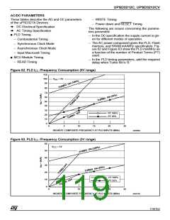
The power and speed of the PLDs are controlled
by the Turbo Bit (Bit 3) in PMMR0 (see Table 79).
By setting the bit to '1,' the Turbo Mode is off and
the PLDs consume the specified standby current
when the inputs are not switching for an extended
time of 70ns. The propagation delay time is in-
creased by 10ns (for a 5V device) after the Turbo
Bit is set to '1' (turned off) when the inputs change
at a composite frequency of less than 15MHz.
When the Turbo Bit is reset to '0' (turned on), the
PLDs run at full power and speed. The Turbo Bit
affects the PLD’s DC power, AC power, and prop-
agation delay. When the Turbo Mode is off, the
uPSD3200 input clock frequency is reduced by
5MHz from the maximum rated clock frequency.
Blocking MCU control signals with the bits of
PMMR2 (see Table 80, page 116) can further re-
duce PLD AC power consumption.
SRAM Standby Mode (Battery Backup). The
SRAM in the PSD MODULE supports a battery
backup mode in which the contents are retained in
the event of a power loss. The SRAM has Voltage
PD2 of Port D can be configured in PSDsoft Ex-
press as PSD Chip Select Input (CSI). When Low,
the signal selects and enables the PSD MODULE
Flash memory, SRAM, and I/O blocks for READ or
WRITE operations. A High on PSD Chip Select In-
put (CSI, PD2) disables the Flash memory, and
SRAM, and reduces power consumption. Howev-
er, the PLD and I/O signals remain operational
when PSD Chip Select Input (CSI, PD2) is High.
Input Clock
CLKIN (PD1) can be turned off, to the PLD to save
AC power consumption. CLKIN (PD1) is an input
to the PLD AND Array and the Output Macrocells
(OMC).
During Power-down Mode, or, if CLKIN (PD1) is
not being used as part of the PLD logic equation,
the clock should be disabled to save AC power.
CLKIN (PD1) is disconnected from the PLD AND
Array or the Macrocells block by setting Bits 4 or 5
to a '1' in PMMR0.
Input Control Signals
The PSD MODULE provides the option to turn off
the MCU signals (WR, RD, PSEN, and Address
Strobe (ALE)) to the PLD to save AC power con-
sumption (see Table 81, page 116). These control
signals are inputs to the PLD AND Array. During
Power-down Mode, or, if any of them are not being
used as part of the PLD logic equation, these con-
trol signals should be disabled to save AC power.
They are disconnected from the PLD AND Array
by setting Bits 2, 3, 4, 5, and 6 to a '1' in PMMR2.
Standby (V
external battery. When V
, PC2) that can be connected to an
STBY
becomes lower than
CC
V
then the SRAM automatically connects to
STBY
Voltage Standby (V
The SRAM Standby Current (I
µA. The SRAM data retention voltage is 2V mini-
mum. The Battery-on Indicator (V ) can be
routed to PC4. This signal indicates when the V
, PC2) as a power source.
STBY
) is typically 0.5
STBY
BATON
CC
has dropped below V
.
STBY
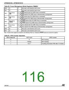
Table 79. Power Management Mode Registers PMMR0
Bit 0
Bit 1
Bit 2
X
0
Not used, and should be set to zero.
0 = off Automatic Power-down (APD) is disabled.
1 = on Automatic Power-down (APD) is enabled.
APD Enable
X
0
Not used, and should be set to zero.
0 = on PLD Turbo Mode is on
Bit 3
PLD Turbo
PLD Turbo Mode is off, saving power.
uPSD3200 operates at 5MHz below the maximum rated clock frequency
1 = off
0 = on
CLKIN (PD1) input to the PLD AND Array is connected. Every change of CLKIN
(PD1) Powers-up the PLD when Turbo Bit is '0.'
Bit 4
Bit 5
PLD Array clk
PLD MCell clk
1 = off CLKIN (PD1) input to PLD AND Array is disconnected, saving power.
0 = on CLKIN (PD1) input to the PLD macrocells is connected.
1 = off CLKIN (PD1) input to PLD macrocells is disconnected, saving power.
Bit 6
Bit 7
X
X
0
0
Not used, and should be set to zero.
Not used, and should be set to zero.
115/152

 STMICROELECTRONICS [ ST ]