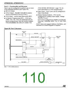
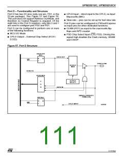
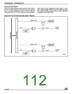
UPSD3212C, UPSD3212CV
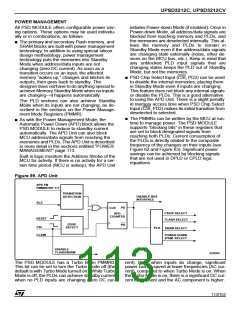
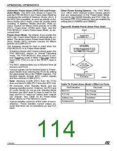
Automatic Power-down (APD) Unit and Power-
down Mode. The APD Unit, shown in Figure 59,
puts the PSD MODULE into Power-down Mode by
monitoring the activity of Address Strobe (ALE). If
the APD Unit is enabled, as soon as activity on Ad-
dress Strobe (ALE) stops, a four-bit counter starts
counting. If Address Strobe (ALE/AS, PD0) re-
mains inactive for fifteen clock periods of CLKIN
(PD1), Power-down (PDN) goes High, and the
PSD MODULE enters Power-down Mode, as dis-
cussed next.
Other Power Saving Options. The PSD MOD-
ULE offers other reduced power saving options
that are independent of the Power-down Mode.
Except for the SRAM Standby and PSD Chip Se-
lect Input (CSI, PD2) features, they are enabled by
setting bits in PMMR0 and PMMR2.
Figure 60. Enable Power-down Flow Chart
RESET
Power-down Mode. By default, if you enable the
APD Unit, Power-down Mode is automatically en-
abled. The device enters Power-down Mode if Ad-
dress Strobe (ALE) remains inactive for fifteen
periods of CLKIN (PD1).
The following should be kept in mind when the
PSD MODULE is in Power-down Mode:
Enable APD
Set PMMR0 Bit 1 = 1
OPTIONAL
Disable desired inputs to PLD
by setting PMMR0 bits 4 and 5
and PMMR2 bits 2 through 6.
– If Address Strobe (ALE) starts pulsing again, the
PSD MODULE returns to normal Operating
mode. The PSD MODULE also returns to nor-
mal Operating mode if either PSD Chip Select
Input (CSI, PD2) is Low or the RESET input is
High.
ALE idle
for 15 CLKIN
clocks?
No
– The MCU address/data bus is blocked from all
memory and PLDs.
– Various signals can be blocked (prior to Power-
down Mode) from entering the PLDs by setting
the appropriate bits in the PMMR registers. The
blocked signals include MCU control signals
and the common CLKIN (PD1).
Yes
PSD Module in Power
Down Mode
AI06609
– Note: Blocking CLKIN (PD1) from the PLDs
does not block CLKIN (PD1) from the APD Unit.
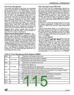
Table 78. Power-down Mode’s Effect on Ports
– All memories enter Standby Mode and are
drawing standby current. However, the PLD and
I/O ports blocks do not go into Standby Mode
because you don’t want to have to wait for the
logic and I/O to “wake-up” before their outputs
can change. See Table 78 for Power-down
Mode effects on PSD MODULE ports.
– Typical standby current is of the order of micro-
amperes. These standby current values as-
sume that there are no transitions on any PLD
input.
Port Function
MCU I/O
Pin Level
No Change
PLD Out
No Change
Undefined
Tri-State
Address Out
Peripheral I/O
114/152

 STMICROELECTRONICS [ ST ]