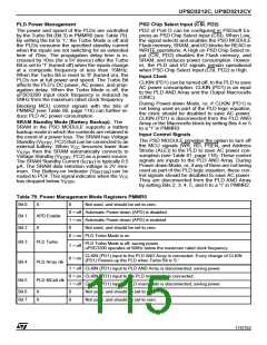
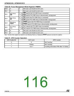
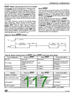
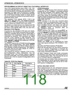
UPSD3212C, UPSD3212CV
AC/DC PARAMETERS
These tables describe the AD and DC parameters
of the uPSD321X Devices:
– WRITE Timing
– Power-down and RESET Timing
➜
➜
DC Electrical Specification
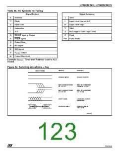
AC Timing Specification
The following are issues concerning the parame-
ters presented:
– In the DC specification the supply current is giv-
en for different modes of operation.
– The AC power component gives the PLD, Flash
memory, and SRAM mA/MHz specification. Fig-
ure 62 and Figure 63 show the PLD mA/MHz as
a function of the number of Product Terms (PT)
used.
– In the PLD timing parameters, add the required
delay when Turbo Bit is '0.'
■ PLD Timing
– Combinatorial Timing
– Synchronous Clock Mode
– Asynchronous Clock Mode
– Input Macrocell Timing
■ MCU Module Timing
– READ Timing
Figure 62. PLD I /Frequency Consumption (5V range)
CC
110
100
90
V
CC
= 5V
80
70
60
50
40
30
20
10
0
PT 100%
PT 25%
0
5
10
15
20
25
HIGHEST COMPOSITE FREQUENCY AT PLD INPUTS (MHz)
AI02894
Figure 63. PLD I /Frequency Consumption (3V range)
CC
60
V
CC
= 3V
50
40
30
20
10
0
PT 100%
PT 25%
0
5
10
15
20
25
HIGHEST COMPOSITE FREQUENCY AT PLD INPUTS (MHz)
AI03100
119/152

 STMICROELECTRONICS [ ST ]