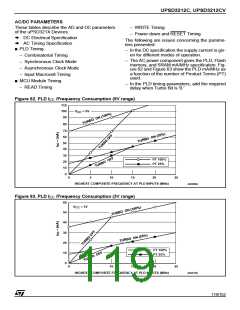
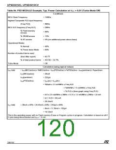
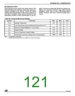
UPSD3212C, UPSD3212CV
PROGRAMMING IN-CIRCUIT USING THE JTAG SERIAL INTERFACE
The JTAG Serial Interface pins (TMS, TCK, TDI,
TDO) are dedicated pins on Port C (see Table 83).
All memory blocks (primary and secondary Flash
memory), PLD logic, and PSD MODULE Configu-
ration Register Bits may be programmed through
the JTAG Serial Interface block. A blank device
can be mounted on a printed circuit board and pro-
grammed using JTAG.
The standard JTAG signals (IEEE 1149.1) are
TMS, TCK, TDI, and TDO. Two additional signals,
TSTAT and TERR, are optional JTAG extensions
used to speed up Program and Erase cycles.
JTAG Extensions
TSTAT and TERR are two JTAG extension signals
enabled by an “ISC_ENABLE” command received
over the four standard JTAG signals (TMS, TCK,
TDI, and TDO). They are used to speed Program
and Erase cycles by indicating status on uPDS
signals instead of having to scan the status out se-
rially using the standard JTAG channel. See Appli-
cation Note AN1153.
TERR indicates if an error has occurred when
erasing a sector or programming a byte in Flash
memory. This signal goes Low (active) when an
Error condition occurs, and stays Low until an
“ISC_CLEAR” command is executed or a chip Re-
set (RESET) pulse is received after an
“ISC_DISABLE” command.
By default, on a blank device (as shipped from the
factory or after erasure), four pins on Port C are
the basic JTAG signals TMS, TCK, TDI, and TDO.
Standard JTAG Signals
TSTAT behaves the same as Ready/Busy de-
scribed in the section entitled “Ready/Busy (PC3),”
page 84. TSTAT is High when the PSD MODULE
device is in READ Mode (primary and secondary
Flash memory contents can be read). TSTAT is
Low when Flash memory Program or Erase cycles
are in progress, and also when data is being writ-
ten to the secondary Flash memory.
At power-up, the standard JTAG pins are inputs,
waiting for a JTAG serial command from an exter-
nal JTAG controller device (such as FlashLINK or
Automated Test Equipment). When the enabling
command is received, TDO becomes an output
and the JTAG channel is fully functional. The
same command that enables the JTAG channel
may optionally enable the two additional JTAG sig-
nals, TSTAT and TERR.
The RESET input to the uPS3200 should be active
during JTAG programming. The active RESET
puts the MCU module into RESET Mode while the
PSD Module is being programmed. See Applica-
tion Note AN1153 for more details on JTAG In-
System Programming (ISP).
TSTAT and TERR can be configured as “open
drain” type signals during an “ISC_ENABLE” com-
mand.
Security and Flash memory Protection
When the Security Bit is set, the device cannot be
read on a Device Programmer or through the
JTAG Port. When using the JTAG Port, only a Full
Chip Erase command is allowed.
All other Program, Erase and Verify commands
are blocked. Full Chip Erase returns the part to a
non-secured blank state. The Security Bit can be
set in PSDsoft Express Configuration.
All primary and secondary Flash memory sectors
can individually be sector protected against era-
sures. The sector protect bits can be set in PSD-
soft Express Configuration.
The uPSD321X Devices supports JTAG In-Sys-
tem-Configuration (ISC) commands, but not
Boundary Scan. The PSDsoft Express software
tool and FlashLINK JTAG programming cable im-
plement the JTAG In-System-Configuration (ISC)
commands.
Table 83. JTAG Port Signals
Port C Pin
PC0
JTAG Signals
TMS
Description
Mode Select
INITIAL DELIVERY STATE
PC1
PC3
PC4
PC5
PC6
TCK
Clock
When delivered from ST, the uPSD321X Devices
have all bits in the memory and PLDs set to '1.'
The code, configuration, and PLD logic are loaded
using the programming procedure. Information for
programming the device is available directly from
ST. Please contact your local sales representa-
tive.
TSTAT
TERR
TDI
Status (optional)
Error Flag (optional)
Serial Data In
Serial Data Out
TDO
118/152

 STMICROELECTRONICS [ ST ]