UPSD3212C, UPSD3212CV
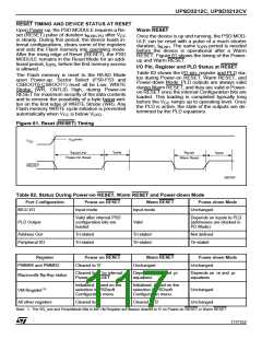
RESET TIMING AND DEVICE STATUS AT RESET
Upon Power-up, the PSD MODULE requires a Re-
Warm RESET
set (RESET) pulse of duration t
after V
NLNH-PO
CC
Once the device is up and running, the PSD MOD-
ULE can be reset with a pulse of a much shorter
is steady. During this period, the device loads in-
ternal configurations, clears some of the registers
and sets the Flash memory into operating mode.
After the rising edge of Reset (RESET), the PSD
MODULE remains in the Reset Mode for an addi-
duration, t
. The same t
period is needed
NLNH
OPR
before the device is operational after a Warm
RESET. Figure 61 shows the timing of the Power-
up and Warm RESET.
tional period, t
is allowed.
, before the first memory access
OPR
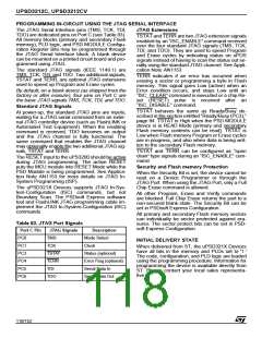
I/O Pin, Register and PLD Status at RESET
Table 82 shows the I/O pin, register and PLD sta-
tus during Power-on RESET, Warm RESET, and
Power-down Mode. PLD outputs are always valid
during Warm RESET, and they are valid in Power-
on RESET once the internal Configuration bits are
loaded. This loading is completed typically long
The Flash memory is reset to the READ Mode
upon Power-up. Sector Select (FS0-FS3 and
CSBOOT0-CSBOOT1) must all be Low, WRITE
Strobe (WR, CNTL0) High, during Power-on
RESET for maximum security of the data contents
and to remove the possibility of a byte being writ-
ten on the first edge of WRITE Strobe (WR). Any
Flash memory WRITE cycle initiation is prevented
before the V ramps up to operating level. Once
CC
the PLD is active, the state of the outputs are de-
termined by the PLD equations.
automatically when V is below V
.
CC
LKO
Figure 61. Reset (RESET) Timing
VCC(min)
V
CC
t
t
OPR
t
t
NLNH-PO
NLNH
Warm Reset
OPR
Power-On Reset
RESET
AI07437
Table 82. Status During Power-on RESET, Warm RESET and Power-down Mode
Port Configuration
MCU I/O
Power-on RESET
Input mode
Warm RESET
Input mode
Power-down Mode
Unchanged
Valid after internal PSD
configuration bits are
loaded
Depends on inputs to PLD
(addresses are blocked in
PD Mode)
PLD Output
Valid
Address Out
Tri-stated
Tri-stated
Tri-stated
Tri-stated
Not defined
Tri-stated
Peripheral I/O
Register
Power-on RESET
Warm RESET
Power-down Mode
PMMR0 and PMMR2
Cleared to '0'
Unchanged
Unchanged
Cleared to '0' by internal
Power-on RESET
Depends on .re and .pr
equations
Depends on .re and .pr
equations
Macrocells flip-flop status
Initialized, based on the
selection in PSDsoft
Configuration menu
Initialized, based on the
selection in PSDsoft
Configuration menu
(1)
Unchanged
Unchanged
VM Register
All other registers
Cleared to '0'
Cleared to '0'
Note: 1. The SR_cod and PeriphMode Bits in the VM Register are always cleared to '0' on Power-on RESET or Warm RESET.
117/152

 STMICROELECTRONICS [ ST ]