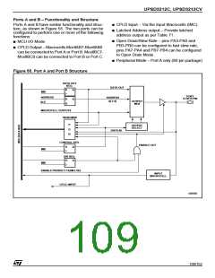
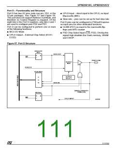
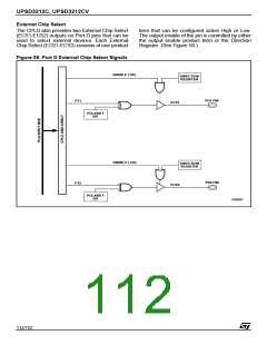
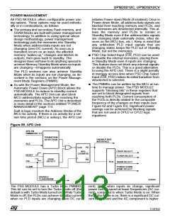
UPSD3212C, UPSD3212CV
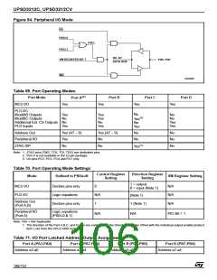
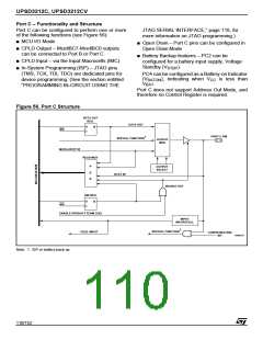
Port C – Functionality and Structure
Port C can be configured to perform one or more
of the following functions (see Figure 56):
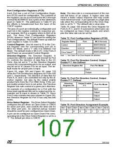
JTAG SERIAL INTERFACE,” page 118, for
more information on JTAG programming.)
■ MCU I/O Mode
■ Open Drain – Port C pins can be configured in
■ CPLD Output – McellBC7-McellBC0 outputs
Open Drain Mode
can be connected to Port B or Port C.
■ Battery Backup features – PC2 can be
■ CPLD Input – via the Input Macrocells (IMC)
configured for a battery input supply, Voltage
Standby (V
).
STBY
■ In-System Programming (ISP) – JTAG pins
(TMS, TCK, TDI, TDO) are dedicated pins for
device programming. (See the section entitled
“PROGRAMMING IN-CIRCUIT USING THE
PC4 can be configured as a Battery-on Indicator
(V ), indicating when V is less than
BATON
CC
V
.
BAT
Port C does not support Address Out Mode, and
therefore no Control Register is required.
Figure 56. Port C Structure
DATA OUT
REG.
DATA OUT
D
Q
WR
PORT C PIN
1
SPECIAL FUNCTION
OUTPUT
MUX
[
]
MCELLBC 7:0
READ MUX
P
D
B
OUTPUT
SELECT
DATA IN
ENABLE OUT
DIR REG.
D
Q
WR
(
)
ENABLE PRODUCT TERM .OE
INPUT
MACROCELL
1
SPECIAL FUNCTION
CPLD-INPUT
CONFIGURATION
BIT
AI06618
Note: 1. ISP or battery back-up
110/152

 STMICROELECTRONICS [ ST ]