UPSD3212C, UPSD3212CV
Port Configuration Registers (PCR)
Each Port has a set of Port Configuration Regis-
ters (PCR) used for configuration. The contents of
the registers can be accessed by the MCU through
normal READ/WRITE bus cycles at the addresses
given in Table 61. The addresses in Table 61 are
the offsets in hexadecimal from the base of the
CSIOP register.
The pins of a port are individually configurable and
each bit in the register controls its respective pin.
For example, Bit 0 in a register refers to Bit 0 of its
port. The three Port Configuration Registers
(PCR), shown in Table 72, are used for setting the
Port configurations. The default Power-up state for
each register in Table 72 is 00h.
Note: The slew rate is a measurement of the rise
and fall times of an output. A higher slew rate
means a faster output response and may create
more electrical noise. A pin operates in a high slew
rate when the corresponding bit in the Drive Reg-
ister is set to '1.' The default rate is slow slew.
Table 76, page 108 shows the Drive Register for
Ports A, B, C, and D. It summarizes which pins can
be configured as Open Drain outputs and which
pins the slew rate can be set for.
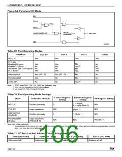
Table 72. Port Configuration Registers (PCR)
Register Name
Control
Port
MCU Access
WRITE/READ
WRITE/READ
WRITE/READ
Control Register. Any bit reset to '0' in the Con-
trol Register sets the corresponding port pin to
MCU I/O Mode, and a '1' sets it to Address Out
Mode. The default mode is MCU I/O. Only Ports A
and B have an associated Control Register.
A,B
Direction
A,B,C,D
A,B,C,D
(1)
Drive Select
Note: 1. See Table 76 for Drive Register Bit definition.
Direction Register. The Direction Register, in
conjunction with the output enable (except for Port
D), controls the direction of data flow in the I/O
Ports. Any bit set to '1' in the Direction Register
causes the corresponding pin to be an output, and
any bit set to '0' causes it to be an input. The de-
fault mode for all port pins is input.
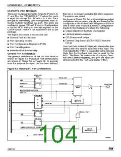
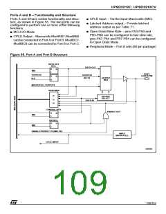
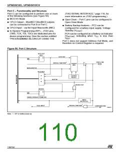
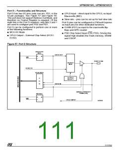
Figure 55, page 109 and Figure 56, page 110
show the Port Architecture diagrams for Ports A/B
and C, respectively. The direction of data flow for
Ports A, B, and C are controlled not only by the di-
rection register, but also by the output enable
product term from the PLD AND Array. If the out-
put enable product term is not active, the Direction
Register has sole control of a given pin’s direction.
Table 73. Port Pin Direction Control, Output
Enable P.T. Not Defined
Direction Register Bit
Port Pin Mode
0
1
Input
Output
Table 74. Port Pin Direction Control, Output
Enable P.T. Defined
Direction
Register Bit
Output Enable
P.T.
Port Pin Mode
0
0
1
1
0
Input
An example of a configuration for a Port with the
three least significant bits set to output and the re-
mainder set to input is shown in Table 75. Since
Port D only contains two pins (shown in Figure 58),
the Direction Register for Port D has only two bits
active.
1
0
1
Output
Output
Output
Drive Select Register. The Drive Select Register
configures the pin driver as Open Drain or CMOS
for some port pins, and controls the slew rate for
the other port pins. An external pull-up resistor
should be used for pins configured as Open Drain.
Table 75. Port Direction Assignment Example
Bit 7 Bit 6 Bit 5 Bit 4 Bit 3 Bit 2 Bit 1 Bit 0
0
0
0
0
0
1
1
1
A pin can be configured as Open Drain if its corre-
sponding bit in the Drive Select Register is set to a
'1.' The default pin drive is CMOS.
107/152

 STMICROELECTRONICS [ ST ]