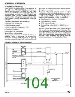
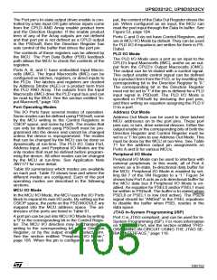
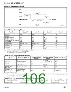
UPSD3212C, UPSD3212CV
Port Data Registers
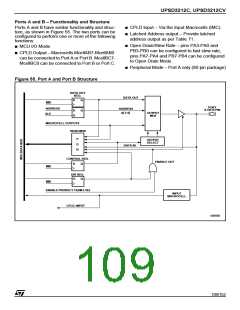
The Port Data Registers, shown in Table 77, are
used by the MCU to write data to or read data from
the ports. Table 77 shows the register name, the
ports having each register type, and MCU access
for each register type. The registers are described
below.
Data In. Port pins are connected directly to the
Data In buffer. In MCU I/O Input Mode, the pin in-
put is read through the Data In buffer.
Register Bits are not set, writing to the macrocell
loads data to the macrocell flip-flops. See the sec-
tion entitled “PLDs,” page 97.
OMC Mask Register. Each OMC Mask Register
Bit corresponds to an Output Macrocell (OMC) flip-
flop. When the OMC Mask Register Bit is set to a
'1,' loading data into the Output Macrocell (OMC)
flip-flop is blocked. The default value is '0' or un-
blocked.
Data Out Register. Stores output data written by
the MCU in the MCU I/O Output Mode. The con-
tents of the Register are driven out to the pins if the
Direction Register or the output enable product
term is set to '1.' The contents of the register can
also be read back by the MCU.
Output Macrocells (OMC). The CPLD Output
Macrocells (OMC) occupy a location in the MCU’s
address space. The MCU can read the output of
the Output Macrocells (OMC). If the OMC Mask
Input Macrocells (IMC). The Input Macrocells
(IMC) can be used to latch or store external inputs.
The outputs of the Input Macrocells (IMC) are rout-
ed to the PLD input bus, and can be read by the
MCU. See the section entitled “PLDs,” page 97.
Enable Out. The Enable Out register can be read
by the MCU. It contains the output enable values
for a given port. A '1' indicates the driver is in out-
put mode. A '0' indicates the driver is in tri-state
and the pin is in input mode.
Table 76. Drive Register Pin Assignment
Drive
Bit 7
Bit 6
Bit 5
Bit 4
Open
Bit 3
Slew
Bit 2
Slew
Bit 1
Slew
Bit 0
Slew
Register
Open
Drain
Open
Drain
Open
Drain
Port A
Drain
Rate
Rate
Rate
Rate
Open
Drain
Open
Drain
Open
Drain
Open
Drain
Slew
Rate
Slew
Rate
Slew
Rate
Slew
Rate
Port B
Port C
Port D
Open
Drain
Open
Drain
Open
Drain
Open
Drain
(1)
(1)
(1)
(1)
NA
NA
NA
NA
Slew
Rate
Slew
Rate
(1)
(1)
(1)
(1)
(1)
(1)
NA
NA
NA
NA
NA
NA
Note: 1. NA = Not Applicable.
Table 77. Port Data Registers
Register Name
Data In
Port
MCU Access
A,B,C,D
READ – input on pin
WRITE/READ
Data Out
A,B,C,D
A,B,C
READ – outputs of macrocells
WRITE – loading macrocells flip-flop
Output Macrocell
Mask Macrocell
WRITE/READ – prevents loading into a given
macrocell
A,B,C
Input Macrocell
Enable Out
A,B,C
A,B,C
READ – outputs of the Input Macrocells
READ – the output enable control of the port driver
108/152

 STMICROELECTRONICS [ ST ]