UPSD3212C, UPSD3212CV
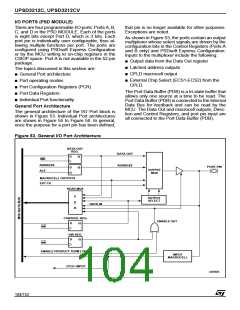
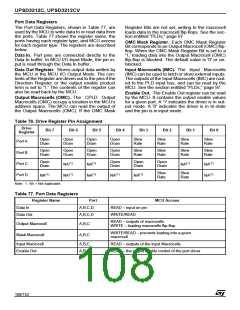
The Port pin’s tri-state output driver enable is con-
trolled by a two input OR gate whose inputs come
from the CPLD AND Array enable product term
and the Direction Register. If the enable product
term of any of the Array outputs are not defined
and that port pin is not defined as a CPLD output
in the PSDsoft, then the Direction Register has
sole control of the buffer that drives the port pin.
put, the content of the Data Out Register drives the
pin. When configured as an input, the MCU can
read the port input through the Data In buffer. See
Figure 53, page 104.
Ports C and D do not have Control Registers, and
are in MCU I/O Mode by default. They can be used
for PLD I/O if equations are written for them in PS-
Dabel.
The contents of these registers can be altered by
the MCU. The Port Data Buffer (PDB) feedback
path allows the MCU to check the contents of the
registers.
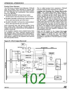
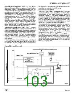
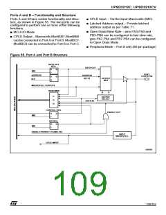
Ports A, B, and C have embedded Input Macro-
cells (IMC). The Input Macrocells (IMC) can be
configured as latches, registers, or direct inputs to
the PLDs. The latches and registers are clocked
by Address Strobe (ALE) or a product term from
the PLD AND Array. The outputs from the Input
Macrocells (IMC) drive the PLD input bus and can
be read by the MCU. See the section entitled “In-
put Macrocell,” page 103.
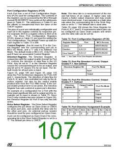
PLD I/O Mode
The PLD I/O Mode uses a port as an input to the
CPLD’s Input Macrocells (IMC), and/or as an out-
put from the CPLD’s Output Macrocells (OMC).
The output can be tri-stated with a control signal.
This output enable control signal can be defined
by a product term from the PLD, or by resetting the
corresponding bit in the Direction Register to '0.'
The corresponding bit in the Direction Register
must not be set to '1' if the pin is defined for a PLD
input signal in PSDsoft. The PLD I/O Mode is
specified in PSDsoft by declaring the port pins,
and then writing an equation assigning the PLD I/
O to a port.
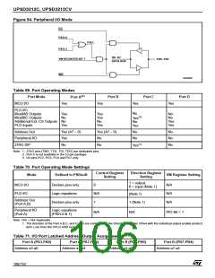
Port Operating Modes
The I/O Ports have several modes of operation.
Some modes can be defined using PSDsoft, some
by the MCU writing to the Control Registers in
CSIOP space, and some by both. The modes that
can only be defined using PSDsoft must be pro-
grammed into the device and cannot be changed
unless the device is reprogrammed. The modes
that can be changed by the MCU can be done so
dynamically at run-time. The PLD I/O, Data Port,
Address Input, and Peripheral I/O Modes are the
only modes that must be defined before program-
ming the device. All other modes can be changed
by the MCU at run-time. See Application Note
AN1171 for more detail.
Address Out Mode
Address Out Mode can be used to drive latched
MCU addresses on to the port pins. These port
pins can, in turn, drive external devices. Either the
output enable or the corresponding bits of both the
Direction Register and Control Register must be
set to a '1' for pins to use Address Out Mode. This
must be done by the MCU at run-time. See Table
71 for the address output pin assignments on
Ports A and B for various MCUs.
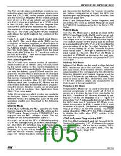
Peripheral I/O Mode
Peripheral I/O Mode can be used to interface with
external peripherals. In this mode, all of Port A
serves as a tri-state, bi-directional data buffer for
the MCU. Peripheral I/O Mode is enabled by set-
ting Bit 7 of the VM Register to a '1.' Figure 54
shows how Port A acts as a bi-directional buffer for
the MCU data bus if Peripheral I/O Mode is en-
abled. An equation for PSEL0 and/or PSEL1 must
be written in PSDsoft. The buffer is tri-stated when
PSEL0 or PSEL1 is low (not active). The PSEN
signal should be “ANDed” in the PSEL equations
to disable the buffer when PSEL resides in the
data space.
Table 69 summarizes which modes are available
on each port. Table 72 shows how and where the
different modes are configured. Each of the port
operating modes are described in the following
sections.
MCU I/O Mode
In the MCU I/O Mode, the MCU uses the I/O Ports
block to expand its own I/O ports. By setting up the
CSIOP space, the ports on the PSD MODULE are
mapped into the MCU address space. The ad-
dresses of the ports are listed in Table 61.
JTAG In-System Programming (ISP)
A port pin can be put into MCU I/O Mode by writing
a '0' to the corresponding bit in the Control Regis-
ter. The MCU I/O direction may be changed by
writing to the corresponding bit in the Direction
Register, or by the output enable product term.
See the section entitled “Peripheral I/O Mode,”
page 105. When the pin is configured as an out-
Port C is JTAG compliant, and can be used for In-
System Programming (ISP). For more information
on the JTAG Port, see the section entitled “PRO-
GRAMMING IN-CIRCUIT USING THE JTAG SE-
RIAL INTERFACE,” page 118.
105/152

 STMICROELECTRONICS [ ST ]