UPSD3212C, UPSD3212CV
The OMC Mask Register. There is one Mask
Register for each of the two groups of eight Output
Macrocells (OMC). The Mask Registers can be
used to block the loading of data to individual Out-
put Macrocells (OMC). The default value for the
Mask Registers is 00h, which allows loading of the
Output Macrocells (OMC). When a given bit in a
Mask Register is set to a '1,' the MCU is blocked
from writing to the associated Output Macrocells
(OMC). For example, suppose McellAB0-
McellAB3 are being used for a state machine. You
would not want a MCU write to McellAB to over-
write the state machine registers. Therefore, you
would want to load the Mask Register for McellAB
(Mask Macrocell AB) with the value 0Fh.
I/O functions. The internal node feedback can be
routed as an input to the AND Array.
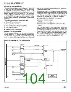
Input Macrocells (IMC)
The CPLD has 20 Input Macrocells (IMC), one for
each pin on Ports A and B, and four on Port C. The
architecture of the Input Macrocells (IMC) is
shown in Figure 52. The Input Macrocells (IMC)
are individually configurable, and can be used as
a latch, register, or to pass incoming Port signals
prior to driving them onto the PLD input bus. The
outputs of the Input Macrocells (IMC) can be read
by the MCU through the internal data bus.
The enable for the latch and clock for the register
are driven by a multiplexer whose inputs are a
product term from the CPLD AND Array or the
MCU Address Strobe (ALE). Each product term
output is used to latch or clock four Input Macro-
cells (IMC). Port inputs 3-0 can be controlled by
one product term and 7-4 by another.
The Output Enable of the OMC. The
Output
Macrocells (OMC) block can be connected to an I/
O port pin as a PLD output. The output enable of
each port pin driver is controlled by a single prod-
uct term from the AND Array, ORed with the Direc-
tion Register output. The pin is enabled upon
Power-up if no output enable equation is defined
and if the pin is declared as a PLD output in PSD-
soft Express.
Configurations for the Input Macrocells (IMC) are
specified by equations written in PSDsoft (see Ap-
plication Note AN1171). Outputs of the Input Mac-
rocells (IMC) can be read by the MCU via the IMC
buffer. See the section entitled “I/O PORTS (PSD
MODULE),” page 104.
If the Output Macrocell (OMC) output is declared
as an internal node and not as a port pin output in
the PSDabel file, the port pin can be used for other
Figure 52. Input Macrocell
[
]
MCU DATA BUS
D 7:0
_
INPUT MACROCELL RD
DIRECTION
REGISTER
(
)
ENABLE .OE
OUTPUT
MACROCELLS BC
PT
AND
MACROCELL AB
I/O PIN
PT
PORT
DRIVER
MUX
Q
D
PT
ALE
MUX
D FF
Q
D
G
FEEDBACK
LATCH
INPUT MACROCELL
AI06603
103/152

 STMICROELECTRONICS [ ST ]