UPSD3212C, UPSD3212CV
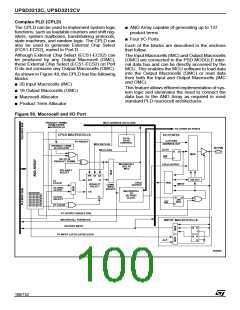
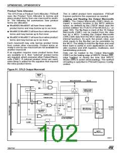
Output Macrocell (OMC)
Eight of the Output Macrocells (OMC) are con-
nected to Ports A and B pins and are named as
McellAB0-McellAB7. The other eight macrocells
are connected to Ports B and C pins and are
named as McellBC0-McellBC7. If an McellAB out-
put is not assigned to a specific pin in PSDsoft, the
Macrocell Allocator block assigns it to either Port A
or B. The same is true for a McellBC output on Port
B or C. Table 68 shows the macrocells and port
assignment.
The Output Macrocell (OMC) architecture is
shown in Figure 51. As shown in the figure, there
are native product terms available from the AND
Array, and borrowed product terms available (if
unused) from other Output Macrocells (OMC). The
polarity of the product term is controlled by the
XOR gate. The Output Macrocell (OMC) can im-
plement either sequential logic, using the flip-flop
element, or combinatorial logic. The multiplexer
selects between the sequential or combinatorial
logic outputs. The multiplexer output can drive a
port pin and has a feedback path to the AND Array
inputs.
The flip-flop in the Output Macrocell (OMC) block
can be configured as a D, T, JK, or SR type in PS-
Dsoft. The flip-flop’s clock, preset, and clear inputs
may be driven from a product term of the AND Ar-
ray. Alternatively, CLKIN (PD1) can be used for
the clock input to the flip-flop. The flip-flop is
clocked on the rising edge of CLKIN (PD1). The
preset and clear are active High inputs. Each clear
input can use up to two product terms.
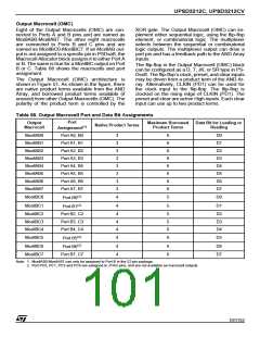
Table 68. Output Macrocell Port and Data Bit Assignments
Port
Output
Macrocell
Maximum Borrowed
Product Terms
Data Bit for Loading or
Reading
Native Product Terms
(1)
Assignment
McellAB0
McellAB1
McellAB2
McellAB3
McellAB4
McellAB5
McellAB6
McellAB7
McellBC0
Port A0, B0
Port A1, B1
Port A2, B2
Port A3, B3
Port A4, B4
Port A5, B5
Port A6, B6
Port A7, B7
3
3
3
3
3
3
3
3
4
6
6
6
6
6
6
6
6
5
D0
D1
D2
D3
D4
D5
D6
D7
D0
(2)
Port B0
(2)
McellBC1
4
5
D1
Port B1
McellBC2
McellBC3
McellBC4
McellBC5
Port B2, C2
Port B3, C3
Port B4, C4
4
4
4
4
5
5
6
6
D2
D3
D4
D5
(2)
Port B5
(2)
McellBC6
McellBC7
4
4
6
6
D6
D7
Port B6
Port B7, C7
Note: 1. McellAB0-McellAB7 can only be assigned to Port B in the 52-pin package.
2. Port PC0, PC1, PC5 and PC6 are assigned to JTAG pins, and are not available as macrocell outputs
101/152

 STMICROELECTRONICS [ ST ]