STM32F405xx, STM32F407xx
Electrical characteristics
(1)(2)
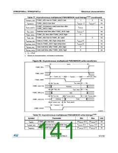
Table 77. Asynchronous multiplexed PSRAM/NOR read timings
(continued)
tv(NADV_NE) FSMC_NEx low to FSMC_NADV low
1
2
ns
tw(NADV)
th(AD_NADV)
th(A_NOE)
FSMC_NADV low time
THCLK– 2
THCLK+1
ns
ns
FSMC_AD(adress) valid hold time after
FSMC_NADV high)
THCLK
-
Address hold time after FSMC_NOE high
THCLK–1
-
-
ns
ns
ns
ns
ns
ns
ns
th(BL_NOE) FSMC_BL time after FSMC_NOE high
tv(BL_NE) FSMC_NEx low to FSMC_BL valid
0
-
2
-
tsu(Data_NE) Data to FSMC_NEx high setup time
tsu(Data_NOE) Data to FSMC_NOE high setup time
th(Data_NE) Data hold time after FSMC_NEx high
th(Data_NOE) Data hold time after FSMC_NOE high
THCLK+4
THCLK+4
-
0
0
-
-
1. CL = 30 pF.
2. Based on characterization, not tested in production.
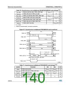
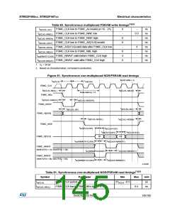
Figure 58. Asynchronous multiplexed PSRAM/NOR write waveforms
t
w(NE)
FSMC_NEx
FSMC_NOE
t
t
t
h(NE_NWE)
v(NWE_NE)
w(NWE)
FSMC_NWE
t
tv(A_NE)
h(A_NWE)
FSMC_A[25:16]
Address
tv(BL_NE)
t
h(BL_NWE)
FSMC_NBL[1:0]
FSMC_AD[15:0]
NBL
t
t
h(Data_NWE)
t
v(A_NE)
v(Data_NADV)
Address
Data
t
th(AD_NADV)
v(NADV_NE)
t
w(NADV)
FSMC_NADV
ai14891B
(1)(2)
Table 78. Asynchronous multiplexed PSRAM/NOR write timings
Symbol
Parameter
FSMC_NE low time
Min
4THCLK–0.5 4THCLK+3
THCLK–0.5 THCLK -0.5
2THCLK–0.5 2THCLK+3
Max
Unit
tw(NE)
tv(NWE_NE)
tw(NWE)
ns
ns
ns
FSMC_NEx low to FSMC_NWE low
FSMC_NWE low tim e
DocID022152 Rev 4
141/185

 STMICROELECTRONICS [ ST ]