STM32F405xx, STM32F407xx
Electrical characteristics
Comments
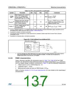
Table 74. DAC characteristics (continued)
Symbol
Parameter
Min Typ
Max
Unit
Max frequency for a correct
DAC_OUT change when
small variation in the input
code (from code i to i+1LSB)
Update
rate(2)
CLOAD ≤ 50 pF,
RLOAD ≥ 5 kΩ
-
-
1
MS/s
CLOAD ≤ 50 pF, RLOAD ≥ 5 kΩ
input code between lowest and
highest possible ones.
Wakeup time from off state
(Setting the ENx bit in the
DAC Control register)
(4)
tWAKEUP
-
-
6.5
10
µs
Power supply rejection ratio
PSRR+ (2) (to VDDA) (static DC
measurement)
–67
–40
dB No RLOAD, CLOAD = 50 pF
1. VDD/VDDA minimum value of 1.7 V is obtained when the device operates in reduced temperature range, and with the use of
an external power supply supervisor (refer to Section : Internal reset OFF).
2. Guaranteed by design, not tested in production.
3. The quiescent mode corresponds to a state where the DAC maintains a stable output level to ensure that no dynamic
consumption occurs.
4. Guaranteed by characterization, not tested in production.
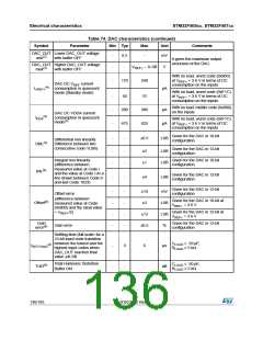
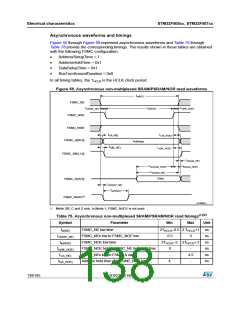
Figure 54. 12-bit buffered /non-buffered DAC
Buffered/Non-buffered DAC
Buffer(1)
R
LOAD
DACx_OUT
12-bit
digital to
analog
converter
C
LOAD
ai17157
1. The DAC integrates an output buffer that can be used to reduce the output impedance and to drive external
loads directly without the use of an external operational amplifier. The buffer can be bypassed by
configuring the BOFFx bit in the DAC_CR register.
5.3.25
FSMC characteristics
Unless otherwise specified, the parameters given in Table 75 to Table 86 for the FSMC
interface are derived from tests performed under the ambient temperature, f
frequency
HCLK
and V supply voltage conditions summarized in Table 14, with the following configuration:
DD
•
•
•
Output speed is set to OSPEEDRy[1:0] = 10
Capacitive load C = 30 pF
Measurement points are done at CMOS levels: 0.5V
DD
Refer to Section Section 5.3.16: I/O port characteristics for more details on the input/output
characteristics.
DocID022152 Rev 4
137/185

 STMICROELECTRONICS [ ST ]