Electrical characteristics
STM32F405xx, STM32F407xx
Asynchronous waveforms and timings
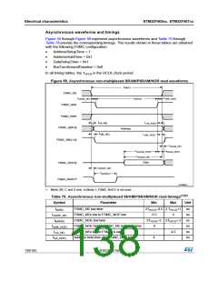
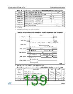
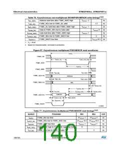
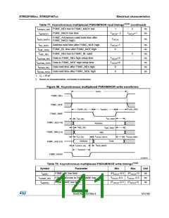
Figure 55 through Figure 58 represent asynchronous waveforms and Table 75 through
Table 78 provide the corresponding timings. The results shown in these tables are obtained
with the following FSMC configuration:
•
•
•
•
AddressSetupTime = 1
AddressHoldTime = 0x1
DataSetupTime = 0x1
BusTurnAroundDuration = 0x0
In all timing tables, the THCLK is the HCLK clock period.
Figure 55. Asynchronous non-multiplexed SRAM/PSRAM/NOR read waveforms
t
w(NE)
FSMC_NE
t
t
t
h(NE_NOE)
w(NOE)
v(NOE_NE)
FSMC_NOE
FSMC_NWE
tv(A_NE)
t
h(A_NOE)
FSMC_A[25:0]
Address
tv(BL_NE)
t
h(BL_NOE)
FSMC_NBL[1:0]
t
h(Data_NE)
t
t
su(Data_NOE)
h(Data_NOE)
t
su(Data_NE)
Data
FSMC_D[15:0]
FSMC_NADV(1)
t
v(NADV_NE)
t
w(NADV)
ai14991c
1. Mode 2/B, C and D only. In Mode 1, FSMC_NADV is not used.
(1)(2)
Table 75. Asynchronous non-multiplexed SRAM/PSRAM/NOR read timings
Symbol
Parameter
FSMC_NE low time
Min
2THCLK–0.5 2 THCLK+1
0.5
2THCLK–2 2THCLK+ 2
Max
Unit
tw(NE)
tv(NOE_NE)
tw(NOE)
ns
ns
ns
ns
ns
ns
FSMC_NEx low to FSMC_NOE low
FSMC_NOE low time
3
th(NE_NOE)
tv(A_NE)
FSMC_NOE high to FSMC_NE high hold time
FSMC_NEx low to FSMC_A valid
Address hold time after FSMC_NOE high
0
-
-
4.5
-
th(A_NOE)
4
138/185
DocID022152 Rev 4

 STMICROELECTRONICS [ ST ]