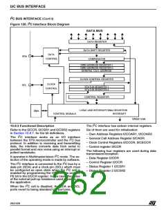
I2C BUS INTERFACE
2
I C BUS INTERFACE (Cont’d)
The following seven registers are used to handle
the interrupt and the DMA features:
bit is set) the General Call address (stored in
I2CADR register). It never recognizes the Start
Byte (address byte 01h) whatever its own address
is.
– Interrupt Status Register I2CISR
– Interrupt Mask Register I2CIMR
– Interrupt Vector Register I2CIVR
Data and addresses are transferred in 8 bits, MSB
first. The first byte(s) following the start condition
contain the address (one byte in 7-bit mode, two
bytes in 10-bit mode). The address is always
transmitted in master mode.
– Receiver DMA Address Pointer Register
I2CRDAP
– Receiver DMA Transaction Counter Register
I2CRDC
A 9th clock pulse follows the 8 clock cycles of a
byte transfer, during which the receiver must send
an acknowledge bit to the transmitter.
Acknowledge is enabled and disabled by software.
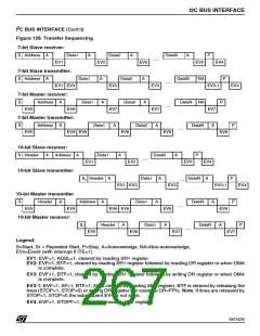
Refer to Figure 127.
– Transmitter DMA Address Pointer Register
I2CTDAP
– Transmitter DMA transaction Counter Register
I2CTDC
The interface can decode both addresses:
– Software programmable 7-bit General Call
address
2
– I C address stored by software in the I2COAR1
register in 7-bit address mode or stored in
I2COAR1 and I2COAR2 registers in 10-bit ad-
dress mode.
After a reset, the interface is disabled.
IMPORTANT:
1. To guarantee correct operation, before enabling
the peripheral (while I2CCR.PE=0), configure bit7
and bit6 of the I2COAR2 register according to the
internal clock INTCLK (for example 11xxxxxxb in
the range 14 - 30 MHz).
2. Bit7 of the I2CCR register must be cleared.
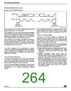
10.8.3.1 Mode Selection
2
In I C mode, the interface can operate in the four
following modes:
– Master transmitter/receiver
– Slave transmitter/receiver
By default, it operates in slave mode.
This interface automatically switches from slave to
master after a start condition is generated on the
bus and from master to slave in case of arbitration
loss or stop condition generation.
In Master mode, it initiates a data transfer and
generates the clock signal. A serial data transfer
always begins with a start condition and ends with
a stop condition. Both start and stop conditions are
generated in master mode by software.
In Slave mode, it is able to recognize its own ad-
dress (7 or 10-bit), as stored in the I2COAR1 and
I2COAR2 registers and (when the I2CCR.ENGC
263/426
9

 STMICROELECTRONICS [ ST ]