SERIAL PERIPHERAL INTERFACE (SPI)
SERIAL PERIPHERAL INTERFACE (Cont’d)
10.7.6 Register Description
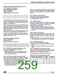
DATA REGISTER (SPDR)
R240 - Read/Write
Note: To use the MISO, MOSI and SCK alternate
functions (input or output), the corresponding I/O
port must be programmed as alternate function
output.
Register Page: 7
Reset Value: 0000 0000 (00h)
7
0
Bit 5 = SPIS Interrupt Selection.
This bit is set and cleared by software.
0: Interrupt source is external interrupt
1: Interrupt source is SPI
D7
D6
D5
D4
D3
D2
D1
D0
The SPDR register is used to transmit and receive
data on the serial bus. In the master device only a
write to this register will initiate transmission/re-
ception of another byte.
Bit 4 = MSTR Master.
This bit is set and cleared by software. It is also
cleared by hardware when, in master mode, SS=0
(see Section 10.7.4.5 Master Mode Fault).
0: Slave mode is selected
Notes: During the last clock cycle the SPIF bit is
set, a copy of the received data byte in the shift
register is moved to a buffer. When the user reads
the serial peripheral data register, the buffer is ac-
tually being read.
1: Master mode is selected, the function of the
SCK pin changes from an input to an output and
the functions of the MISO and MOSI pins are re-
versed.
Warning: A write to the SPDR register places data
directly into the shift register for transmission.
Bit 3 = CPOL Clock polarity.
A read to the SPDR register returns the value lo-
cated in the buffer and not the content of the shift
register (see Figure 121).
This bit is set and cleared by software. This bit de-
termines the steady state of the serial Clock. The
CPOL bit affects both the master and slave
modes.
0: The steady state is a low value at the SCK pin.
1: The steady state is a high value at the SCK pin.
CONTROL REGISTER (SPCR)
R241 - Read/Write
Register Page: 7
Bit 2 = CPHA Clock phase.
This bit is set and cleared by software.
0: The first clock transition is the first data capture
edge.
Reset Value: 0000 0000 (00h)
7
0
SPIE SPOE SPIS MSTR CPOL CPHA SPR1 SPR0
1: The second clock transition is the first capture
edge.
Bit 7 = SPIE Serial peripheral interrupt enable.
This bit is set and cleared by software.
0: Interrupt is inhibited
1: An SPI interrupt is generated whenever either
SPIF or MODF are set in the SPSR register
while the other flag is 0.
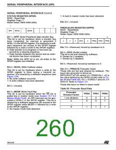
Bit 1:0 = SPR[1:0] Serial peripheral rate.
These bits are set and cleared by software. They
select one of four baud rates to be used as the se-
rial clock when the device is a master.
These 2 bits have no effect in slave mode.
Table 49. Serial Peripheral Baud Rate
Bit 6 = SPOE Serial peripheral output enable.
This bit is set and cleared by software. It is also
cleared by hardware when, in master mode, SS=0
(see Section 10.7.4.5 Master Mode Fault).
0: SPI alternate functions disabled (MISO, MOSI
and SCK can only work as input)
1: SPI alternate functions enabled (MISO, MOSI
and SCK can work as input or output depending
on the value of MSTR)
INTCLK Clock Divide
SPR1
SPR0
2
4
16
32
0
0
1
1
0
1
0
1
259/426
9

 STMICROELECTRONICS [ ST ]