I2C BUS INTERFACE
2
I C BUS INTERFACE (Cont’d)
2
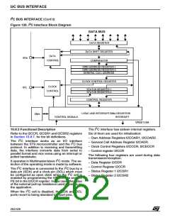
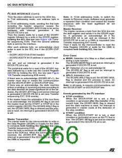
Figure 126. I C Interface Block Diagram
DATA BUS
DATA REGISTER
DATA SHIFT REGISTER
COMPARATOR
DATA
SDA
CONTROL
OWN ADDRESS REGISTER 1
OWN ADDRESS REGISTER 2
GENERAL CALL ADDRESS
CLOCK CONTROL REGISTER
CLOCK
SCL
STATUS REGISTER 1
STATUS REGISTER 2
CONTROL
CONTROL REGISTER
LOGIC AND INTERRUPT/DMA REGISTERS
INTERRUPT
DMA
CONTROL SIGNALS
VR02119A
2
10.8.3 Functional Description
The I C interface has sixteen internal registers.
Six of them are used for initialization:
– Own Address Registers I2COAR1, I2COAR2
– General Call Address Register I2CADR
– Clock Control Registers I2CCCR, I2CECCR
– Control register I2CCR
Refer to the I2CCR, I2CSR1 and I2CSR2 registers
in Section 10.8.7. for the bit definitions.
2
The I C interface works as an I/O interface
2
between the ST9 microcontroller and the I C bus
protocol. In addition to receiving and transmitting
data, the interface converts data from serial to
parallel format and vice versa using an interrupt or
polled handshake.
The following four registers are used during data
transmission/reception:
2
It operates in Multimaster/slave I C mode. The se-
– Data Register I2CDR
lection of the operating mode is made by software.
– Control Register I2CCR
– Status Register 1 I2CSR1
– Status Register 2 I2CSR2
2
2
The I C interface is connected to the I C bus by a
data pin (SDA) and a clock pin (SCL) which must
2
be configured as open drain when the I C cell is
enabled by programming the I/O port bits and the
PE bit in the I2CCR register. In this case, the value
of the external pull-up resistance used depends on
the application.
2
When the I C cell is disabled, the SDA and SCL
ports revert to being standard I/O port pins.
262/426
9

 STMICROELECTRONICS [ ST ]