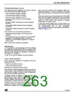
SERIAL PERIPHERAL INTERFACE (SPI)
SERIAL PERIPHERAL INTERFACE (Cont’d)
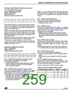
STATUS REGISTER (SPSR)
R242 - Read Only
1: A fault in master mode has been detected
Bits 3:0 = Unused.
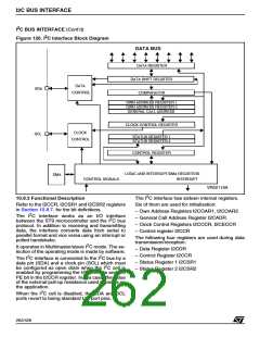
Register Page: 7
Reset Value: 0000 0000 (00h)
7
0
-
PRESCALER REGISTER (SPPR)
R243 - Read/Write
Register Page: 7
Reset Value: 0000 0000 (00h)
SPIF
WCOL
-
MODF
-
-
-
Bit 7 = SPIF Serial Peripheral data transfer flag.
This bit is set by hardware when a transfer has
been completed. An interrupt is generated if
SPIE=1 in the SPCR register. It is cleared by a soft-
ware sequence (an access to the SPSR register
followed by a read or write to the SPDR register).
0: Data transfer is in progress or has been ap-
proved by a clearing sequence.
7
0
0
0
0
DIV2
0
PRS2 PRS1 PRS0
Bits 7:5 = Reserved, forced by hardware to 0.
Bit 4 = DIV2 Divider enable.
This bit is set and cleared by software.
0: Divider by 2 enabled.
1: Data transfer between the device and an exter-
nal device has been completed.
1: Divider by 2 disabled.
Note: While the SPIF bit is set, all writes to the
SPDR register are inhibited.
Bit 3 = Reserved. forced by hardware to 0.
Bit 6 = WCOL Write Collision status.
Bits 2:0 = PRS[2:0] Prescaler Value.
This bit is set by hardware when a write to the
SPDR register is done during a transmit se-
quence. It is cleared by a software sequence (see
Figure 124).
0: No write collision occurred
1: A write collision has been detected
These bits are set and cleared by software. The
baud rate generator is driven by
INTCLK/(n1*n2*n3) where n1= PRS[2:0]+1, n2 is
the value defined by the SPR[1:0] bits (refer to Ta-
ble 49 and Table 50), n3 = 1 if DIV2=1 and n3= 2 if
DIV2=0. Refer to Figure 121.
These bits have no effect in slave mode.
Table 50. Prescaler Baud Rate
Prescaler
Bit 5 = Unused.
Bit 4 = MODF Mode Fault flag.
PRS2
PRS1 PRS0
This bit is set by hardware when the SS pin is
pulled low in master mode (see Section 10.7.4.5
Master Mode Fault). An SPI interrupt can be gen-
erated if SPIE=1 in the SPCR register. This bit is
cleared by a software sequence (An access to the
SPSR register while MODF=1 followed by a write
to the SPCR register).
Division Factor
1 (no division)
0
0
0
0
0
1
2
...
8
1
1
1
0: No master mode fault detected
260/426
9

 STMICROELECTRONICS [ ST ]