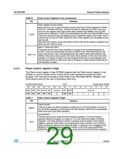
ST10F276E
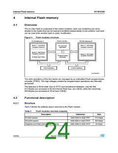
Internal Flash memory
4.2.2
Modules structure
The IFLASH module is composed of two banks. Bank 0 contains 384 Kbyte of program
memory divided in 10 sectors. Bank 0 contains also a reserved sector named test-Flash.
Bank 1 contains 128 Kbyte of program memory or parameter divided in two sectors
(64 Kbyte each).
The XFLASH module is composed of two banks as well. Bank 2 contains 192 Kbyte of
program memory divided in three sectors. Bank 3 contains 128 Kbyte of program memory
or parameter divided in two sectors (64 Kbyte each).
Addresses from 0x0E 0000 to 0x0E FFFF are reserved for the control register interface and
other internal service memory space used by the Flash program/erase controller.
The following tables show the memory mapping of the Flash when it is accessed in read
mode (Table 3), and when accessed in write or erase mode (Table 2): note that with this
second mapping, the first three banks are remapped into code segment 1 (same as
obtained when setting bit ROMS1 in SYSCON register).
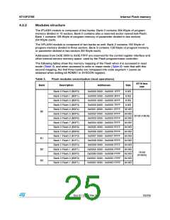
Table 3.
Bank
Flash modules sectorization (read operations)
ST10 bus
size
Description
Addresses
Size
Bank 0 Flash 0 (B0F0)
Bank 0 Flash 1 (B0F1)
Bank 0 Flash 2 (B0F2)
Bank 0 Flash 3 (B0F3)
Bank 0 Flash 4 (B0F4)
Bank 0 Flash 5 (B0F5)
Bank 0 Flash 6 (B0F6)
Bank 0 Flash 7 (B0F7)
Bank 0 Flash 8 (B0F8)
Bank 0 Flash 9 (B0F9)
Bank 1 Flash 0 (B1F0)
Bank 1 Flash 1 (B1F1)
Bank 2 Flash 0 (B2F0)
Bank 2 Flash 1 (B2F1)
Bank 2 Flash 2 (B2F2)
Bank 3 Flash 0 (B3F0)
Bank 3 Flash 1 (B3F1)
0x0000 0000 - 0x0000 1FFF
0x0000 2000 - 0x0000 3FFF
0x0000 4000 - 0x0000 5FFF
0x0000 6000 - 0x0000 7FFF
0x0001 8000 - 0x0001 FFFF
0x0002 0000 - 0x0002 FFFF
0x0003 0000 - 0x0003 FFFF
0x0004 0000 - 0x0004 FFFF
0x0005 0000 - 0x0005 FFFF
0x0006 0000 - 0x0006 FFFF
0x0007 0000 - 0x0007 FFFF
0x0008 0000 - 0x0008 FFFF
0x0009 0000 - 0x0009 FFFF
0x000A 0000 - 0x000A FFFF
0x000B 0000 - 0x000B FFFF
0x000C 0000 - 0x000C FFFF
0x000D 0000 - 0x000D FFFF
8 KB
8 KB
8 KB
8 KB
32 KB
64 KB
64 KB
64 KB
64 KB
64 KB
64 KB
64 KB
64 KB
64 KB
64 KB
64 KB
64 KB
B0
32-bit (I-BUS)
B1
B2
B3
16-bit
(X-BUS)
Doc ID 12303 Rev 3
25/235

 STMICROELECTRONICS [ ST ]