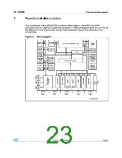
ST10F276E
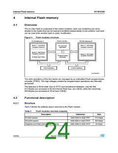
Internal Flash memory
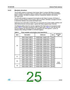
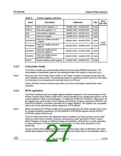
Table 5.
Bank
Control register interface
Description
ST10
Size
Addresses
bus size
FCR1-0
FDR1-0
FAR
Flash control registers 1-0
Flash data registers 1-0
Flash address registers
Flash error register
0x000E 0000 - 0x000E 0007
0x000E 0008 - 0x000E 000F
0x000E 0010 - 0x000E 0013
0x000E 0014 - 0x000E 0015
8 byte
8 byte
4 byte
2 byte
FER
Flash non-volatile protection
X register
FNVWPXR
FNVWPIR
FNVAPR0
0x000E DFB0 - 0x000E DFB3 4 byte
0x000E DFB4 - 0x000E DFB7 4 byte
0x000E DFB8 - 0x000E DFB9 2 byte
0x000E DFBC - 0x000E DFBF 4 byte
16-bit
(X-BUS)
Flash non-volatile protection
I register
Flash non-volatile access
protection register 0
Flash non-volatile access
protection register 1
FNVAPR1
XFICR
XFlash interface control register
0x000E E000 - 0x000E E001
2 byte
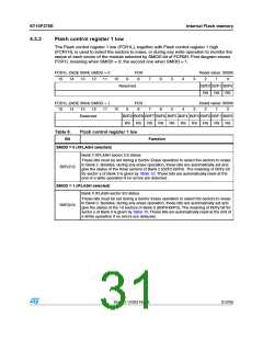
4.2.3
Low power mode
The Flash modules are automatically switched off executing PWRDN instruction. The
consumption is drastically reduced, but exiting this state can require a long time (tPD).
Note:
Recovery time from Power Down mode for the Flash modules is anyway shorter than the
main oscillator start-up time. To avoid any problem in restarting to fetch code from the Flash,
it is important to size properly the external circuit on RPD pin.
Power-off Flash mode is entered only at the end of the eventually running Flash write
operation.
4.2.4
Write operation
The Flash modules have one single register interface mapped in the memory space of the
XFlash module (0x0E 0000 to 0x0E 0013). All the operations are enabled through four 16-bit
control registers: Flash Control Register 1-0 High/Low (FCR1H/L-FCR0H/L). Eight other 16-
bit registers are used to store Flash Address and Data for Program operations (FARH/L and
FDR1H/L-FDR0H/L) and Write Operation Error flags (FERH/L). All registers are accessible
with 8 and 16-bit instructions (since mapped on ST10 XBUS).
Note:
Before accessing the XFlash module (and consequently also the Flash register to be used
for program/erasing operations), bit XFLASHEN in XPERCON register and bit XPEN in
SYSCON register shall be set.
The four banks have their own dedicated sense amplifiers, so that any bank can be read
while any other bank is written. However simultaneous write operations (“write” means
either Program or Erase) on different banks are forbidden: when there is a write operation
on going (Program or Erase) anywhere in the Flash, no other write operation can be
performed.
During a Flash write operation any attempt to read the bank under modification will output
invalid data (software trap 009Bh). This means that the Flash bank is not fetchable when a
Doc ID 12303 Rev 3
27/235

 STMICROELECTRONICS [ ST ]