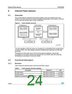
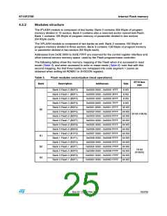
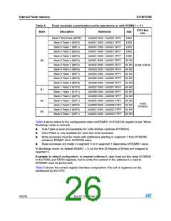
Internal Flash memory
ST10F276E
write operation is active: the write operation commands must be executed from another
bank, or from the other module or again from another memory (internal RAM or external
memory).
Note:
During a Write operation, when bit LOCK of FCR0 is set, it is forbidden to write into the
Flash Control Registers.
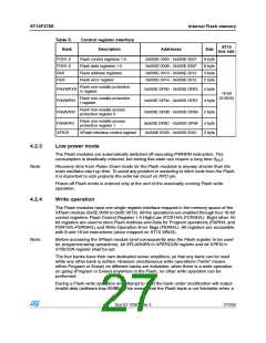
4.2.5
Power supply drop
If during a write operation the internal low voltage supply drops below a certain internal
voltage threshold, any write operation running is suddenly interrupted and the modules are
reset to Read mode. At following Power-on, an interrupted Flash write operation must be
repeated.
4.3
Registers description
4.3.1
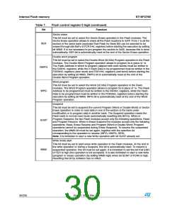
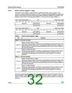
Flash control register 0 low
The Flash control register 0 low (FCR0L) together with the Flash control register 0 high
(FCR0H) is used to enable and to monitor all the write operations for both the Flash
modules. The user has no access in write mode to the test-Flash (B0TF). Besides, test-
Flash block is seen by the user in Bootstrap mode only.
FCR0L (0x0E 0000)
15 14 13
FCR
8
Reset value: 0000h
12
11
10
9
7
6
5
4
3
2
1
0
Reserved
BSY1 BSY0 LOCK Res. BSY3 BSY2 Res.
R
R
R
R
R
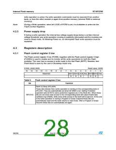
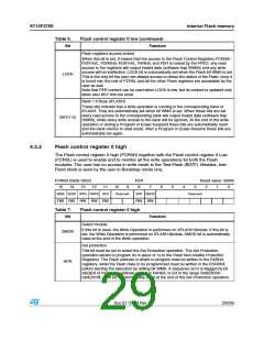
Table 6.
Bit
Flash control register 0 low
Function
Bank 3:2 Busy (XFLASH)
These bits indicate that a write operation is running on the corresponding bank of
XFLASH. They are automatically set when bit WMS is set. Setting Protection
operation sets bit BSY2 (since protection registers are in the Block B2). When these
bits are set every read access to the corresponding bank will output invalid data
(software trap 009Bh), while every write access to the bank will be ignored. At the end
of the write operation or during a Program or Erase Suspend these bits are
automatically reset and the bank returns to read mode. After a Program or Erase
Resume these bits are automatically set again.
BSY(3:2)
28/235
Doc ID 12303 Rev 3

 STMICROELECTRONICS [ ST ]