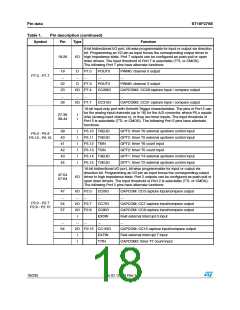
Pin data
Table 1.
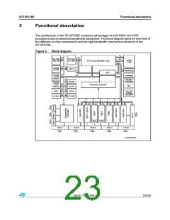
ST10F276E
Pin description (continued)
Symbol
Pin
Type
Function
XTAL1
XTAL2
138
137
I
XTAL1 Main oscillator amplifier circuit and/or external clock input.
XTAL2 Main oscillator amplifier circuit output.
O
To clock the device from an external source, drive XTAL1 while leaving XTAL2
unconnected. Minimum and maximum high / low and rise / fall times specified in
the AC Characteristics must be observed.
XTAL3
XTAL4
143
144
I
XTAL3 32 kHz oscillator amplifier circuit input
XTAL4 32 kHz oscillator amplifier circuit output
O
When 32 kHz oscillator amplifier is not used, to avoid spurious consumption,
XTAL3 shall be tied to ground while XTAL4 shall be left open. Besides, bit OFF32
in RTCCON register shall be set. 32 kHz oscillator can only be driven by an
external crystal, and not by a different clock source.
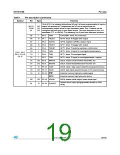
Reset Input with CMOS Schmitt-Trigger characteristics. A low level at this pin for
a specified duration while the oscillator is running resets the ST10F276E. An
internal pull-up resistor permits power-on reset using only a capacitor connected
to VSS. In bidirectional reset mode (enabled by setting bit BDRSTEN in
SYSCON register), the RSTIN line is pulled low for the duration of the internal
reset sequence.
RSTIN
140
141
I
Internal Reset Indication Output. This pin is driven to a low level during
hardware, software or watchdog timer reset. RSTOUT remains low until the EINIT
(end of initialization) instruction is executed.
RSTOUT
O
Non-Maskable Interrupt Input. A high to low transition at this pin causes the CPU
to vector to the NMI trap routine. If bit PWDCFG = ‘0’ in SYSCON register, when
the PWRDN (power down) instruction is executed, the NMI pin must be low in
order to force the ST10F276E to go into power down mode. If NMI is high and
PWDCFG = ‘0’, when PWRDN is executed, the part will continue to run in
normal mode.
NMI
142
I
If not used, pin NMI should be pulled high externally.
VAREF
VAGND
37
38
-
-
A/D converter reference voltage and analog supply
A/D converter reference and analog ground
Timing pin for the return from interruptible power down mode and synchronous /
asynchronous reset selection.
RPD
84
-
17, 46,
72,82,93,
109, 126,
136
Digital supply voltage = + 5V during normal operation, idle and power down
modes.
It can be turned off when Stand-by RAM mode is selected.
VDD
-
18,45,
55,71,
83,94,
110, 127,
139
VSS
-
-
Digital ground
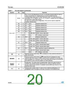
1.8V decoupling pin: a decoupling capacitor (typical value of 10nF, max 100nF)
must be connected between this pin and nearest VSS pin.
V18
56
22/235
Doc ID 12303 Rev 3

 STMICROELECTRONICS [ ST ]