Internal Flash memory
ST10F276E
4
Internal Flash memory
4.1
Overview
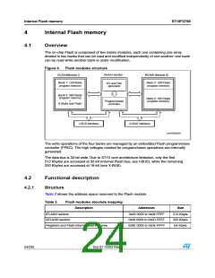
The on-chip Flash is composed of two matrix modules, each one containing one array
divided in two banks that can be read and modified independently of one another: one bank
can be read while another bank is under modification.
Figure 4.
Flash modules structure
#ONTROL SECTION
)&,!3(ꢍ-ODULE )ꢏ
8&,!3( ꢍ-ODULE 8ꢏ
"ANK ꢀꢐ ꢀꢁꢆ +BYTE
PROGRAM MEMORY
"ANK ꢈꢐ ꢀꢁꢆ +BYTE
PROGRAM MEMORY
(6 AND 2EFꢌ
GENERATOR
"ANK ꢉꢐ ꢈꢆꢇ +BYTE
PROGRAM MEMORY
ꢑ
"ANK ꢁꢐ ꢀꢋꢁ +BYTE
PROGRAM MEMORY
0ROGRAMꢂERASE
CONTROLLER
ꢆ +BYTE TESTꢅ&LASH
)ꢅ"53 INTERFACE
8ꢅ"53 INTERFACE
'!0'2)ꢉꢉꢈꢁꢀ
The write operations of the four banks are managed by an embedded Flash program/erase
controller (FPEC). The high voltages needed for program/erase operations are internally
generated.
The data bus is 32-bit wide. Due to ST10 core architecture limitation, only the first
512 Kbytes are accessed at 32-bit (internal Flash bus, see I-BUS), while the remaining
320 Kbytes are accessed at 16-bit (see X-BUS).
4.2
Functional description
4.2.1
Structure
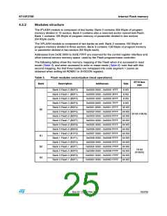
Table 2 shows the address space reserved to the Flash module.
Table 2.
Flash modules absolute mapping
Description
Addresses
Size
IFLASH sectors
0x00 0000 to 0x08 FFFF
0x09 0000 to 0x0D FFFF
0x0E 0000 to 0x0E FFFF
512 Kbyte
320 Kbyte
64 Kbyte
XFLASH sectors
Registers and Flash internal reserved area
24/235
Doc ID 12303 Rev 3

 STMICROELECTRONICS [ ST ]