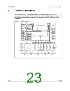
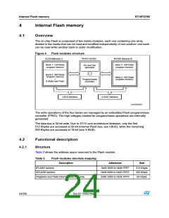
ST10F276E
Pin data
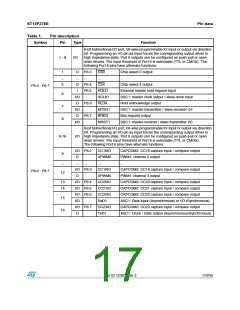
Table 1.
Symbol
Pin description (continued)
Pin
Type
Function
External access enable pin.
A low level applied to this pin during and after Reset forces the ST10F276E to
start the program from the external memory space. A high level forces
ST10F276E to start in the internal memory space. This pin is also used (when
Stand-by mode is entered, that is ST10F276E under reset and main VDD turned
off) to bias the 32 kHz oscillator amplifier circuit and to provide a reference
voltage for the low-power embedded voltage regulator which generates the
internal 1.8V supply for the RTC module (when not disabled) and to retain data
inside the Stand-by portion of the XRAM (16 Kbyte).
EA / VSTBY
99
I
It can range from 4.5 to 5.5V (6V for a reduced amount of time during the device
life, 4.0V when RTC and 32 kHz on-chip oscillator amplifier are turned off). In
running mode, this pin can be tied low during reset without affecting 32 kHz
oscillator, RTC and XRAM activities, since the presence of a stable VDD
guarantees the proper biasing of all those modules.
Two 8-bit bidirectional I/O ports P0L and P0H, bit-wise programmable for input or
output via direction bit. Programming an I/O pin as input forces the
corresponding output driver to high impedance state. The input threshold of
Port 0 is selectable (TTL or CMOS).
In case of an external bus configuration, PORT0 serves as the address (A) and
as the address / data (AD) bus in multiplexed bus modes and as the data (D) bus
in demultiplexed bus modes.
Demultiplexed bus modes
P0L.0 -P0L.7, 100-107,
P0H.0 108,
P0H.1 - P0H.7 111-117
Data path width
P0L.0 – P0L.7:
P0H.0 – P0H.7:
8-bit
16-bi
I/O
D0 – D7
I/O
D0 - D7
D8 - D15
Multiplexed bus modes
Data path width
P0L.0 – P0L.7:
P0H.0 – P0H.7:
8-bit
16-bi
AD0 – AD7
A8 – A15
AD0 - AD7
AD8 - AD15
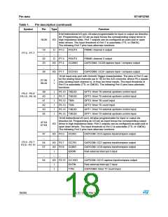
Two 8-bit bidirectional I/O ports P1L and P1H, bit-wise programmable for input or
output via direction bit. Programming an I/O pin as input forces the
corresponding output driver to high impedance state. PORT1 is used as the 16-
bit address bus (A) in demultiplexed bus modes: if at least BUSCONx is
configured such the demultiplexed mode is selected, the pis of PORT1 are not
available for general purpose I/O function. The input threshold of Port 1 is
selectable (TTL or CMOS).
118-125
128-135
I/O
The pins of P1L also serve as the additional (up to 8) analog input channels for
the A/D converter, where P1L.x equals ANy (Analog input channel y,
where y = x + 16). This additional function have higher priority on demultiplexed
bus function. The following PORT1 pins have alternate functions:
P1L.0 - P1L.7
P1H.0 - P1H.7
132
133
134
135
I
I
I
I
P1H.4 CC24IO
P1H.5 CC25IO
P1H.6 CC26IO
P1H.7 CC27IO
CAPCOM2: CC24 capture input
CAPCOM2: CC25 capture input
CAPCOM2: CC26 capture input
CAPCOM2: CC27 capture input
Doc ID 12303 Rev 3
21/235

 STMICROELECTRONICS [ ST ]