ST10F276E
Internal Flash memory
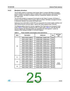
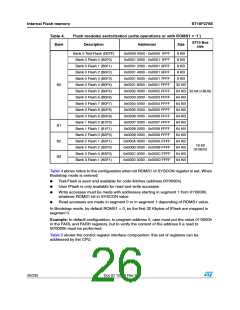
Table 6.
Bit
Flash control register 0 low (continued)
Function
Flash registers access locked
When this bit is set, it means that the access to the Flash Control Registers FCR0H/-
FCR1H/L, FDR0H/L-FDR1H/L, FARH/L and FER is locked by the FPEC: any read
access to the registers will output invalid data (software trap 009Bh) and any write
access will be ineffective. LOCK bit is automatically set when the Flash bit WMS is set.
This is the only bit the user can always access to detect the status of the Flash: once it
is found low, the rest of FCR0L and all the other Flash registers are accessible by the
user as well.
LOCK
Note that FER content can be read when LOCK is low, but its content is updated only
when also BSY bits are reset.
Bank 1:0 Busy (IFLASH)
These bits indicate that a write operation is running in the corresponding bank of
IFLASH. They are automatically set when bit WMS is set. When these bits are set
every read access to the corresponding bank will output invalid data (software trap
009Bh), while every write access to the bank will be ignored. At the end of the write
operation or during a Program or Erase Suspend these bits are automatically reset
and the bank returns to read mode. After a Program or Erase Resume these bits are
automatically set again.
BSY(1:0)
4.3.2
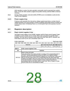
Flash control register 0 high
The Flash control register 0 high (FCR0H) together with the Flash control register 0 Low
(FCR0L) is used to enable and to monitor all the write operations for both the Flash
modules. The user has no access in write mode to the Test-Flash (B0TF). Besides, test-
Flash block is seen by the user in Bootstrap mode only.
FCR0H (0x0E 0002)
15 14 13
FCR
8
Reset value: 0000h
12
11
10
9
7
6
5
4
3
2
1
0
WMS SUSP WPG DWPG SER
Reserved
SPR SMOD
Reserved
RW RW RW RW RW
RW RW
Table 7.
Bit
Flash control register 0 high
Function
Select module
If this bit is reset, the Write Operation is performed on XFLASH Module; if this bit is
set, the Write Operation is performed on IFLASH Module. SMOD bit is automatically
reset at the end of the Write operation.
SMOD
Set protection
This bit must be set to select the Set Protection operation. The Set Protection
operation allows to program 0s in place of 1s in the Flash Non-volatile Protection
Registers. The Flash Address in which to program must be written in the FARH/L
registers, while the Flash Data to be programmed must be written in the FDR0H/L
before starting the execution by setting bit WMS. A sequence error is flagged by bit
SEQER of FER if the address written in FARH/L is not in the range 0x0EDFB0-
0x0EDFBF. SPR bit is automatically reset at the end of the Set Protection operation.
SPR
Doc ID 12303 Rev 3
29/235

 STMICROELECTRONICS [ ST ]